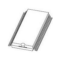
PCF8576CT NXP Semiconductors, PCF8576CT Datasheet - Page 19

PCF8576CT
Manufacturer Part Number
PCF8576CT
Description
Manufacturer
NXP Semiconductors
Datasheet
1.PCF8576CT.pdf
(56 pages)
Specifications of PCF8576CT
Operating Supply Voltage (typ)
2.5/3.3/5V
Number Of Digits
20
Number Of Segments
160
Package Type
VSO
Pin Count
56
Mounting
Surface Mount
Power Dissipation
400mW
Frequency (max)
315KHz
Operating Supply Voltage (min)
2V
Operating Supply Voltage (max)
6V
Lead Free Status / Rohs Status
Compliant
Available stocks
Company
Part Number
Manufacturer
Quantity
Price
Part Number:
PCF8576CT
Manufacturer:
PHILIPS/飞利浦
Quantity:
20 000
Part Number:
PCF8576CT/1
Manufacturer:
NXP/恩智浦
Quantity:
20 000
Part Number:
PCF8576CT/1,518
Manufacturer:
NXP/恩智浦
Quantity:
20 000
Company:
Part Number:
PCF8576CT/1112
Manufacturer:
NXP Semiconductors
Quantity:
135
Company:
Part Number:
PCF8576CT/1118
Manufacturer:
NXPSemicondu
Quantity:
2 802
Company:
Part Number:
PCF8576CT/1Ј¬112
Manufacturer:
NXP
Quantity:
880
Company:
Part Number:
PCF8576CT/1Ј¬118
Manufacturer:
NXP
Quantity:
21 000
Part Number:
PCF8576CT/F1
Manufacturer:
PHILIPS/飞利浦
Quantity:
20 000
Part Number:
PCF8576CTT
Manufacturer:
NXP/恩智浦
Quantity:
20 000
NXP Semiconductors
PCF8576C_9
Product data sheet
When display data is transmitted to the PCF8576C, the display bytes received are stored
in the display RAM in accordance with the selected LCD drive mode. The data is stored as
it arrives and does not wait for an acknowledge cycle as with the commands. Depending
on the current multiplex drive mode, data is stored singularly, in pairs, triplets or
quadruplets. To illustrate the filling order, an example of a 7-segment numeric display
showing all drive modes is given in
applies equally to other LCD types.
The following applies to
Fig 12. Display RAM bit map
•
•
•
•
In the static drive mode, the eight transmitted data bits are placed in row 0 of eight
successive 4-bit RAM words.
In the 1:2 multiplex mode, the eight transmitted data bits are placed in pairs into
row 0 and 1 of four successive 4-bit RAM words.
In the 1:3 multiplex mode, the eight bits are placed in triples into row 0, 1 and 2 to
three successive 4-bit RAM words, with bit 3 of the third address left unchanged. It is
not recommended to use this bit in a display because of the difficult addressing. This
last bit may, if necessary, be controlled by an additional transfer to this address but
care should be taken to avoid overwriting adjacent data because always full bytes are
transmitted.
In the 1:4 multiplex mode, the eight transmitted data bits are placed in quadruples into
row 0, 1, 2 and 3 of two successive 4-bit RAM words.
backplane outputs
display RAM bits
Display RAM bit map showing direct relationship between RAM addresses and segment outputs;
also between bits in a RAM word and the backplane outputs.
(rows)/
(BP)
0
1
2
3
Rev. 09 — 9 July 2009
Figure
0
1
13:
2
display RAM addresses (columns)/segment outputs (S)
Figure
3
4
13; the RAM filling organization depicted
Universal LCD driver for low multiplex rates
35
PCF8576C
36
© NXP B.V. 2009. All rights reserved.
37
38
mbe525
39
19 of 56


