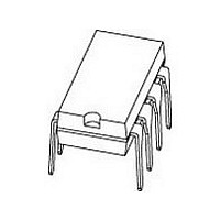
TDA7052A NXP Semiconductors, TDA7052A Datasheet - Page 6

TDA7052A
Manufacturer Part Number
TDA7052A
Description
Manufacturer
NXP Semiconductors
Datasheet
1.TDA7052A.pdf
(14 pages)
Specifications of TDA7052A
Operational Class
Class-AB
Audio Amplifier Output Configuration
1-Channel Mono
Output Power (typ)
1.1x1@8OhmW
Audio Amplifier Function
Speaker
Total Harmonic Distortion
0.3@8Ohm@500mW%
Single Supply Voltage (typ)
5/9/12/15V
Dual Supply Voltage (typ)
Not RequiredV
Power Supply Requirement
Single
Power Dissipation
1.25W
Rail/rail I/o Type
No
Power Supply Rejection Ratio
46dB
Single Supply Voltage (min)
4.5V
Single Supply Voltage (max)
18V
Dual Supply Voltage (min)
Not RequiredV
Dual Supply Voltage (max)
Not RequiredV
Operating Temp Range
-40C to 85C
Operating Temperature Classification
Industrial
Mounting
Through Hole
Pin Count
8
Package Type
PDIP
Lead Free Status / Rohs Status
Compliant
Available stocks
Company
Part Number
Manufacturer
Quantity
Price
Company:
Part Number:
TDA7052A
Manufacturer:
PHILIPS
Quantity:
654
Company:
Part Number:
TDA7052A
Manufacturer:
NXPL
Quantity:
4 770
Company:
Part Number:
TDA7052A
Manufacturer:
TOS
Quantity:
4 780
Part Number:
TDA7052A
Manufacturer:
PHILIPS/飞利浦
Quantity:
20 000
Company:
Part Number:
TDA7052A/B
Manufacturer:
HARR
Quantity:
68
Part Number:
TDA7052A/N2,112
Manufacturer:
NXP/恩智浦
Quantity:
20 000
Company:
Part Number:
TDA7052AT
Manufacturer:
AMD
Quantity:
6 218
Part Number:
TDA7052AT
Manufacturer:
PHILIPS/飞利浦
Quantity:
20 000
Part Number:
TDA7052AT/N2
Manufacturer:
NXP/恩智浦
Quantity:
20 000
NXP Semiconductors
CHARACTERISTICS
V
Notes to the characteristics
1. With a load connected to the outputs the quiescent current will increase, the maximum value of this increase being
2. The noise output voltage (RMS value) at f = 500 kHz is measured with R
3. The ripple rejection is measured with R
4. The noise output voltage (RMS value) is measured with R
July 1994
V
I
Maximum gain; V
P
THD
G
V
V
B
SVRR
|V
Z
Minimum gain; V
G
V
Mute position
V
DC volume control
φ
I
P
P
4
SYMBOL
I
P
O
I
no(rms)
no(rms)
O
1 W BTL mono audio amplifier with DC
volume control
v
v
off
= 6 V; T
equal to the DC output offset voltage dividend by R
is applied to the positive supply rail.
|
amb
positive supply voltage range
total quiescent current
output power
total harmonic distortion
voltage gain
input signal handling
noise output voltage (RMS value)
bandwidth
supply voltage ripple rejection
DC output offset voltage
input impedance (pin 2)
voltage gain
noise output voltage (RMS value)
output voltage in mute position
gain control range
control current
= 25 °C; f = 1 kHz; TDA7052A: R
TDA7052A
TDA7052AT
TDA7052A
TDA7052AT
4
4
= 0.5 V
= 1.4 V
PARAMETER
S
= 0 Ω and f = 100 Hz to 10 kHz. The ripple voltage of 200 mV, (RMS value)
L
= 8 Ω; TDA7052AT: R
V
note 1
THD = 10%
P
P
V
f = 500 kHz; note 2
−1 dB
note 3
note 4
V
V
P
O
O
4
4
4
L
= 0.8 V; THD < 1%
≤ 0.3 V; V
= 0.4 V
= 6 V; R
= 0.5 W
= 0.25 W
.
6
CONDITIONS
S
= 5 kΩ unweighted.
L
= ∞
I
= 600 mV
L
= 16 Ω; unless otherwise specified (see Fig.6).
S
= 0 Ω and bandwidth = 5 kHz.
4.5
−
1.0
0.5
−
−
34.5
0.5
−
−
38
−
15
−
−
−
75
60
MIN.
−
7
1.1
0.55
0.3
0.3
35.5
0.65
210
20 Hz to
300 kHz
46
0
20
−44
20
−
80
70
TDA7052A/AT
TYP.
Product specification
18
12
−
−
1
1
36.5
−
−
−
−
150
25
−
30
30
−
80
MAX. UNIT
V
mA
W
W
%
%
dB
V
μV
dB
mV
kΩ
dB
μV
μV
dB
μA


