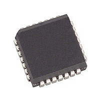
SL811HST Cypress Semiconductor Corp, SL811HST Datasheet - Page 5

SL811HST
Manufacturer Part Number
SL811HST
Description
Manufacturer
Cypress Semiconductor Corp
Datasheet
1.SL811HST.pdf
(32 pages)
Specifications of SL811HST
Operating Temperature (min)
0C
Operating Temperature Classification
Commercial
Package Type
PLCC
Rad Hardened
No
Lead Free Status / Rohs Status
Not Compliant
Available stocks
Company
Part Number
Manufacturer
Quantity
Price
Company:
Part Number:
SL811HST
Manufacturer:
CYP
Quantity:
3 000
Company:
Part Number:
SL811HST
Manufacturer:
CYPRESS
Quantity:
3 000
Company:
Part Number:
SL811HST
Manufacturer:
CYPRESS
Quantity:
5
Part Number:
SL811HST
Manufacturer:
CYPRESS/赛普拉斯
Quantity:
20 000
Company:
Part Number:
SL811HST-1.5
Manufacturer:
CYP
Quantity:
2 340
Part Number:
SL811HST-1.5
Manufacturer:
CYPRESS/赛普拉斯
Quantity:
20 000
Company:
Part Number:
SL811HST-AC
Manufacturer:
Cypress Semiconductor Corp
Quantity:
10 000
Company:
Part Number:
SL811HST-AXC
Manufacturer:
Cypress Semiconductor Corp
Quantity:
10 000
Part Number:
SL811HST-AXC
Manufacturer:
CYPRESS/赛普拉斯
Quantity:
20 000
3.1.2.2 USB-A/USB-B Host Control Registers [Address = 00h, 08h]
Table 3-3. USB-A/USB-B Host Control Register Definition [Address 00h, 08h]
Once the other SL811HS control registers are configured
(registers 01h-04h or 09h-0Ch) the Host control register is
programmed to initiate the USB transfer. This register will
3.1.2.3 USB-A/USB-B Host Base Address [Address = 01h, 09h]
Table 3-4. USB-A/USB-B Host Base Address Definition [Address 01h, 09h]
The USB-A/B Base Address is a pointer to the SL811HS memory buffer location for USB reads and writes. When transferring
data OUT (Host to Device), the USB-A and USB-B Host Base Address Registers can be set up prior to setting ARM on the USB-
A or USB-B Host Control register. When using a double buffer scheme the Host Base Address could be set up with the first buffer
being used for DATA0 data and the other for DATA1 data.
Document 38-08008 Rev. *B
Bit Position
Preamble
HBADD7
Bit 7
Bit 7
7
6
5
4
3
2
1
0
Bit Name
Preamble
Data Toggle Bit
SyncSOF
ISO
Reserved
Direction
Enable
Arm
Data Toggle Bit
HBADD6
Bit 6
Bit 6
SyncSOF
HBADD5
Function
If bit = “1” a preamble token is transmitted prior to transfer of low-speed packet. If bit = “0,”
preamble generation is disabled.
“0” if DATA0, “1” if DATA1 (only used for OUT tokens in host mode).
“1” = Synchronize with the SOF transfer when operating in FS only.
The SL811HS uses bit 5 to enable transfer of a data packet after a SOF packet is transmitted.
When bit 5 = 1, the next enabled packet will be sent after next SOF. If bit 5 = 0 the next
packet is sent immediately if the SIE is free. If operating in low-speed, do not set this bit.
When set to “1” allows Isochronous mode for this packet.
Bit 3 is reserved for future usage.
When equal to “1” transmit (OUT). When equal to “0” receive (IN).
If Enable = “1”, allows transfers to occur. If Enable = “0”, USB transactions are ignored. The
Enable bit is used in conjunction with the Arm bit (bit 0 of this register) for USB transfers.
Allows enabled transfers when Arm = “1.” Cleared to “0” when transfer is complete (when
Done Interrupt is asserted).
Bit 5
Bit 5
• The SL811HS automatically generates preamble packets when bit 7 is set. This bit is only
• When SL811HS communicates directly to low-speed device:
used to send packets to a low-speed device through a hub. To communicate to a full
speed device, this bit is set to zero. For example, when SL811HS communicates to a
low-speed device via the HUB:
— SL811HS SIE should be set to operate at full-speed, i.e., bit 5 of register 05h (Control
— Bit 6 of register 0Fh (Control Register 2) should be set = “0,” set correct polarity of
— Bit 7, Preamble Bit, should be set = “1” in Host Control register.
— Bit 5 of register 05h (Control Register 1) should be set = “1.”
— Bit 6 of register 0Fh (Control Register 2) should be set = “1,” DATA+ and DATA– polarity
— The state of bit 7 is ignored in this mode.
Register 1) should be equal to “0.”
DATA+ and DATA– state for Full Speed.
for low speed.
HBADD4
Bit 4
Bit 4
ISO
initiate the transfer when the Enable and Arm bit are set as
described above.
Reserved
HBADD3
Bit 3
Bit 3
HBADD2
Direction
Bit 2
Bit 2
HBADD1
Enable
Bit 1
Bit 1
SL811HS
Page 5 of 32
HBADD0
Bit 0
Bit 0
Arm
[+] Feedback


