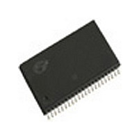
CY7C1021BV33L-12ZC Cypress Semiconductor Corp, CY7C1021BV33L-12ZC Datasheet - Page 3

CY7C1021BV33L-12ZC
Manufacturer Part Number
CY7C1021BV33L-12ZC
Description
Manufacturer
Cypress Semiconductor Corp
Datasheet
1.CY7C1021BV33L-12ZC.pdf
(11 pages)
Specifications of CY7C1021BV33L-12ZC
Density
1Mb
Access Time (max)
12ns
Sync/async
Asynchronous
Architecture
Not Required
Clock Freq (max)
Not RequiredMHz
Operating Supply Voltage (typ)
3.3V
Address Bus
16b
Package Type
TSOP-II
Operating Temp Range
0C to 70C
Number Of Ports
1
Supply Current
150mA
Operating Supply Voltage (min)
2.97V
Operating Supply Voltage (max)
3.63V
Operating Temperature Classification
Commercial
Mounting
Surface Mount
Pin Count
44
Word Size
16b
Number Of Words
64K
Lead Free Status / Rohs Status
Not Compliant
Available stocks
Company
Part Number
Manufacturer
Quantity
Price
Part Number:
CY7C1021BV33L-12ZC
Manufacturer:
CYPRESS/赛普拉斯
Quantity:
20 000
AC Test Loads and Waveforms
Electrical Characteristics
Capacitance
Document #: 38-05148 Rev. *A
OUTPUT
Parameter
V
V
V
V
I
I
I
I
I
Shaded areas contain advance information.
IX
OZ
CC
SB1
SB2
C
C
Note:
3.
OH
OL
IH
IL
Equivalent to: THÉVENIN
IN
OUT
INCLUDING
JIG AND
SCOPE
3.3V
Tested initially and after any design or process changes that may affect these parameters.
Parameter
30 pF
Output HIGH
Voltage
Output LOW
Voltage
Input HIGH
Voltage
Input LOW
Voltage
Input Load
Current
Output Leakage
Current
V
Supply Current
Automatic CE
Power-Down
Current
—TTL Inputs
Automatic CE
Power-Down
Current
—CMOS Inputs
CC
Description
[3]
(a)
EQUIVALENT
Operating
R 317
[2]
Input Capacitance
Output Capacitance
351
OUTPUT
R2
V
I
V
GND < V
GND < V
Output Disabled
V
I
f = f
Max. V
CE > V
V
V
Max. V
CE > V
V
or V
f = 0
OH
OUT
CC
CC
CC
IN
IN
IN
Description
Over the Operating Range
Test Conditions
OUTPUT
MAX
> V
< V
> V
= –4.0 mA
IN
= Min., I
= Min.,
= Max.,
= 0 mA,
< 0.3V,
CC
CC
IH
CC
INCLUDING
JIG AND
SCOPE
IH
IL
CC
3.3V
= 1/t
, f = f
I
I
,
,
or
< V
< V
– 0.3V,
– 0.3V,
OL
RC
CC
CC
MAX
30 pF
167
= 8.0 mA
5 pF
,
Com
Ind
L
(b)
R 317
T
7C1021BV-8 7C1021BV-10
Min.
A
2.4
2.2
0.3
= 25°C, f = 1 MHz
1
1
1.73V
351
R2
V
Max.
0.3V
Test Conditions
170
190
500
0.4
0.8
CC
+1
+1
40
5
+
GND
3.0V
Rise Time: 1 V/ns
Min.
2.4
2.2
0.3
1
1
V
Max.
0.3V
160
120
500
0.4
0.8
CC
+1
+1
40
5
+
10%
7C1021BV-12 7C1021BV-15
Min.
–0.3
2.4
2.2
90%
–1
–1
ALL INPUT PULSES
CY7C1021BV33
Max.
V
Max.
0.3V
150
170
500
0.4
0.8
6
8
+1
+1
40
CC
5
+
Min.
–0.3
2.4
2.2
–1
–1
Fall Time: 1 V/ns
90%
V
Page 3 of 11
Max.
0.3V
140
160
500
0.4
0.8
CC
+1
+1
40
Unit
5
pF
pF
10%
+
Unit
mA
mA
mA
mA
V
V
V
V
A
A
A
[+] Feedback


