74LVC1G07GW NXP Semiconductors, 74LVC1G07GW Datasheet - Page 11
74LVC1G07GW
Manufacturer Part Number
74LVC1G07GW
Description
Manufacturer
NXP Semiconductors
Datasheet
1.74LVC1G07GW.pdf
(17 pages)
Specifications of 74LVC1G07GW
Logic Family
LVC
Logical Function
Buffer/Driver
Number Of Elements
1
Number Of Channels
1
Number Of Inputs
1
Number Of Outputs
1
Operating Supply Voltage (typ)
1.8/2.5/3.3/5V
Package Type
TSSOP
Output Type
Open Drain
Polarity
Non-Inverting
Propagation Delay Time
8.4ns
Low Level Output Current
32mA
Operating Supply Voltage (max)
5.5V
Operating Supply Voltage (min)
1.65V
Quiescent Current
200uA
Technology
CMOS
Pin Count
5
Mounting
Surface Mount
Operating Temp Range
-40C to 125C
Operating Temperature Classification
Automotive
Lead Free Status / Rohs Status
Compliant
Available stocks
Company
Part Number
Manufacturer
Quantity
Price
Company:

Part Number:
74LVC1G07GW
Manufacturer:
NXP
Quantity:
6 000
Part Number:
74LVC1G07GW
Manufacturer:
PH
Quantity:
20 000
Company:
Part Number:
74LVC1G07GW,125
Manufacturer:
NXP Semiconductors
Quantity:
4 600


NXP Semiconductors
Fig 12. Package outline SOT891 (XSON6)
74LVC1G07
Product data sheet
XSON6: plastic extremely thin small outline package; no leads; 6 terminals; body 1 x 1 x 0.5 mm
DIMENSIONS (mm are the original dimensions)
Note
1. Can be visible in some manufacturing processes.
UNIT
mm
VERSION
OUTLINE
SOT891
max
0.5
A
max
0.04
A
1
0.20
0.12
e
b
terminal 1
index area
6×
IEC
(1)
L
1.05
0.95
1
D
1.05
0.95
E
0
1
6
JEDEC
0.55
e
All information provided in this document is subject to legal disclaimers.
e
1
REFERENCES
D
0.35
2
5
e
1
Rev. 9 — 24 August 2010
e
1
0.35
0.27
L
b
3
4
JEITA
0.40
0.32
scale
L
1
1
A
1
E
L
A
4×
(1)
2 mm
PROJECTION
Buffer with open-drain output
EUROPEAN
74LVC1G07
© NXP B.V. 2010. All rights reserved.
ISSUE DATE
05-04-06
07-05-15
SOT891
11 of 17
Related parts for 74LVC1G07GW
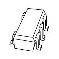
Image
Part Number
Description
Manufacturer
Datasheet
Request
R

Part Number:
Description:
TXRX 8BIT DUAL CONF VOLT 24TSSOP
Manufacturer:
Fairchild Semiconductor
Datasheet:

Part Number:
Description:
TXRX 8BIT DUAL CONF VOLT 24SOIC
Manufacturer:
Fairchild Semiconductor
Datasheet:

Part Number:
Description:
TXRX 8BIT DUAL CONF VOLT 24QSOP
Manufacturer:
Fairchild Semiconductor
Datasheet:
Part Number:
Description:
TXRX 8BIT DUAL CONF VOLT 24QSOP
Manufacturer:
Fairchild Semiconductor
Datasheet:

Part Number:
Description:
IC SWITCH QUAD 1X2 14TSSOP
Manufacturer:
NXP Semiconductors
Datasheet:

Part Number:
Description:
IC MUX/DEMUX DUAL 4X1 16SSOP
Manufacturer:
NXP Semiconductors
Datasheet:

Part Number:
Description:
IC MUX/DEMUX 8X1 16TSSOP
Manufacturer:
NXP Semiconductors
Datasheet:
Part Number:
Description:
IC MUX/DEMUX DUAL 4X1 16TSSOP
Manufacturer:
NXP Semiconductors
Datasheet:
Part Number:
Description:
IC MUX/DEMUX TRIPLE 2X1 16TSSOP
Manufacturer:
NXP Semiconductors
Datasheet:

Part Number:
Description:
IC MUX/DEMUX 8X1 16SOIC
Manufacturer:
NXP Semiconductors
Datasheet:
Part Number:
Description:
IC MUX/DEMUX 8X1 16SSOP
Manufacturer:
NXP Semiconductors
Datasheet:
Part Number:
Description:
IC MUX/DEMUX DUAL 4X1 16SOIC
Manufacturer:
NXP Semiconductors
Datasheet:
Part Number:
Description:
IC MUX/DEMUX TRIPLE 2X1 16SOIC
Manufacturer:
NXP Semiconductors
Datasheet:
Part Number:
Description:
IC MUX/DEMUX TRIPLE 2X1 16SSOP
Manufacturer:
NXP Semiconductors
Datasheet:

Part Number:
Description:
IC SWITCH QUAD 1X2 14SOIC
Manufacturer:
NXP Semiconductors
Datasheet: