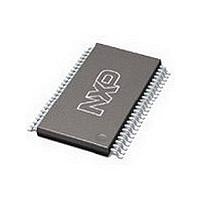
74LVC16244ADGG NXP Semiconductors, 74LVC16244ADGG Datasheet - Page 9

74LVC16244ADGG
Manufacturer Part Number
74LVC16244ADGG
Description
Manufacturer
NXP Semiconductors
Datasheet
1.74LVC16244ADGG.pdf
(19 pages)
Specifications of 74LVC16244ADGG
Logic Family
LVC
Logical Function
Buffer/Line Driver
Number Of Elements
4
Number Of Channels
16
Number Of Inputs
16
Number Of Outputs
16
Operating Supply Voltage (typ)
1.8/2.5/3.3V
Package Type
TSSOP
Output Type
3-State
Polarity
Non-Inverting
Propagation Delay Time
8ns
High Level Output Current
-24mA
Low Level Output Current
24mA
Operating Supply Voltage (max)
3.6V
Operating Supply Voltage (min)
1.2V
Quiescent Current
80uA
Technology
CMOS
Pin Count
48
Mounting
Surface Mount
Operating Temp Range
-40C to 125C
Operating Temperature Classification
Automotive
Lead Free Status / Rohs Status
Compliant
Available stocks
Company
Part Number
Manufacturer
Quantity
Price
Company:
Part Number:
74LVC16244ADGG
Manufacturer:
NXP
Quantity:
2 270
Part Number:
74LVC16244ADGG
Manufacturer:
NXP/恩智浦
Quantity:
20 000
Part Number:
74LVC16244ADGGR
Manufacturer:
PHILIPS/飞利浦
Quantity:
20 000
Company:
Part Number:
74LVC16244ADGGRG4
Manufacturer:
NXP
Quantity:
1 700
Company:
Part Number:
74LVC16244ADGGЈ¬118
Manufacturer:
NXP
Quantity:
2 000
NXP Semiconductors
Table 7.
Voltages are referenced to GND (ground = 0 V). For test circuit see
[1]
[2]
[3]
11. Waveforms
74LVC_LVCH16244A_9
Product data sheet
Symbol Parameter
C
Fig 7.
PD
t
t
t
Typical values are measured at T
C
P
f
C
V
N = number of inputs switching
Σ(C
pd
en
dis
i
D
CC
PD
= input frequency in MHz; f
L
is the same as t
is the same as t
= output load capacitance in pF
= C
is the same as t
L
is used to determine the dynamic power dissipation (P
= supply voltage in Volts
× V
power
dissipation
capacitance
Measurement points are given in
Logic levels: V
The input (nAn) to output (nYn) propagation delays
PD
Dynamic characteristics
CC
× V
2
× f
CC
o
2
) = sum of the outputs.
× f
PLH
PZL
PLZ
i
× N + Σ(C
OL
and t
and t
and t
and V
Conditions
per buffer; V
outputs enabled
outputs disabled
PZH
PHL
PHZ
o
= output frequency in MHz
OH
L
.
.
.
× V
amb
are typical output voltage levels that occur with the output load.
CC
nYn output
= 25 °C and V
nAn input
2
…continued
I
× f
= GND to V
Table
o
All information provided in this document is subject to legal disclaimers.
) where:
GND
V
V
8.
OH
OL
V
I
CC
Rev. 09 — 18 March 2010
t
PLH
CC
74LVC16244A; 74LVCH16244A
= 3.3 V.
; V
CC
D
16-bit buffer/line driver; 5 V input/output tolerant; 3-state
V
in μW).
M
= 3.3 V
V
M
Figure
[3]
Min
9.
-
-
−40 °C to +85 °C
V
M
V
M
t
PHL
mna171
Typ
4.0
12
Max
-
-
−40 °C to +125 °C Unit
Min
-
-
© NXP B.V. 2010. All rights reserved.
Max
-
-
9 of 19
pF
pF


