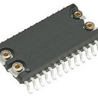
M48T18-100MH1 STMicroelectronics, M48T18-100MH1 Datasheet - Page 9

M48T18-100MH1
Manufacturer Part Number
M48T18-100MH1
Description
RAM Miscellaneous 8KX8 TIMEKEEP 100NS
Manufacturer
STMicroelectronics
Datasheet
1.M48T18-100MH1.pdf
(31 pages)
Specifications of M48T18-100MH1
Bus Type
Parallel
Date Format
DW:DM:M:Y
Time Format
HH:MM:SS
User Ram
8KB
Operating Supply Voltage (typ)
5V
Package Type
SOH
Operating Supply Voltage (max)
5.5V
Operating Supply Voltage (min)
4.5V
Operating Temperature Classification
Commercial
Operating Temperature (max)
70C
Operating Temperature (min)
0C
Pin Count
28
Mounting
Surface Mount
Lead Free Status / Rohs Status
Not Compliant
Available stocks
Company
Part Number
Manufacturer
Quantity
Price
Part Number:
M48T18-100MH1
Manufacturer:
ST
Quantity:
20 000
Part Number:
M48T18-100MH1TR
Manufacturer:
ST
Quantity:
20 000
M48T08, M48T08Y, M48T18
2.1
Figure 5.
Note:
A0-A12
E1
E2
G
DQ0-DQ7
READ mode
The M48T08/18/08Y is in the READ mode whenever W (WRITE enable) is high, E1 (chip
enable 1) is low, and E2 (chip enable 2) is high. The device architecture allows ripple-
through access of data from eight of 65,536 locations in the static storage array. Thus, the
unique address specified by the 13 address inputs defines which one of the 8,192 bytes of
data is to be accessed. Valid data will be available at the data I/O pins within address access
time (t
access times are also satisfied. If the E1, E2 and G access times are not met, valid data will
be available after the latter of the chip enable access times (t
enable access time (t
The state of the eight three-state data I/O signals is controlled by E1, E2 and G. If the
outputs are activated before t
until t
will remain valid for output data hold time (t
address access.
READ mode AC waveforms
WRITE enable (W) = high.
AVQV
AVQV
. If the address inputs are changed while E1, E2 and G remain active, output data
) after the last address input signal is stable, providing that the E1, E2, and G
GLQV
tE2HQX
tE1LQX
tAVQV
tE2HQV
tE1LQV
tGLQX
).
tGLQV
AVQV
Doc ID 2411 Rev 10
, the data lines will be driven to an indeterminate state
VALID
tAVAV
AXQX
) but will go indeterminate until the next
VALID
tGHQZ
E1LQV
or t
E2HQV
Operation modes
tAXQX
tE1HQZ
tE2LQZ
) or output
AI00962
9/31


