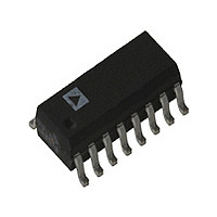
AD8803AR-REEL Analog Devices Inc, AD8803AR-REEL Datasheet - Page 12

AD8803AR-REEL
Manufacturer Part Number
AD8803AR-REEL
Description
Manufacturer
Analog Devices Inc
Datasheet
1.AD8803AR-REEL.pdf
(16 pages)
Specifications of AD8803AR-REEL
Number Of Channels
8
Resolution
8b
Conversion Rate
1.7MSPS
Interface Type
Serial (3-Wire/SPI)
Single Supply Voltage (typ)
3/5V
Dual Supply Voltage (typ)
Not RequiredV
Settling Time
0.6us
Architecture
R-2R
Power Supply Requirement
Single
Output Type
Voltage
Integral Nonlinearity Error
±1.5LSB
Single Supply Voltage (min)
2.7V
Single Supply Voltage (max)
5.5V
Dual Supply Voltage (min)
Not RequiredV
Dual Supply Voltage (max)
Not RequiredV
Operating Temp Range
-40C to 85C
Operating Temperature Classification
Industrial
Mounting
Surface Mount
Pin Count
16
Package Type
SOIC N
Lead Free Status / Rohs Status
Not Compliant
AD8801/AD8803
Unlike the serial port interface of Figure 25, the parallel port in-
terface only transmits 11 bits to the AD8801/AD8803. Also, the
BYTESWAP subroutine is not required for the parallel inter-
face, because data can be shifted out MSB first. However, the
results of the two interface methods are exactly identical. In
most cases, the decision on which method to use will be deter-
mined by whether or not the serial data port is available for
communication with the AD8801/AD8803.
An MC68HC11-to-AD8801/AD8803 Interface
Like the 8051, the MC68HC11 includes a dedicated serial data
port (labeled SPI). The SPI port provides an easy interface to
the AD8801/AD8803 (Figure 27). The interface uses three lines
of Port D for the serial data, and one or two lines from Port C
to control the SHDN and RS (AD8801 only) inputs.
Figure 26. An AD8801/AD8803-8051 C Interface Using
Parallel Port 1
PORT 1
8051 µC
1.7
1.6
1.5
1.4
P1.7
P1.6
P1.5
P1.4
SDI
CLK
CS
SHDN
V
GND
+5V
AD8803
DD
V
V
REFH
REFL
O1
O2
O3
O4
O5
O6
O7
O8
–12–
A software routine for loading the AD8801/AD8803 from a
68HC11 evaluation board is shown in Listing 3. First, the
MC68HC11 is configured for SPI operation. Bits CPHA and
CPOL define the SPI mode wherein the serial clock (SCK) is
high at the beginning and end of transmission, and data is valid
on the rising edge of SCK. This mode matches the requirements
of the AD8801/AD8803. After the registers are saved on the
stack, the DAC value and address are transferred to RAM and
the AD8801/AD8803’s CS is driven low. Next, the DAC’s ad-
dress byte is transferred to the SPDR register, which automati-
cally initiates the SPI data transfer. The program tests the SPIF
bit and loops until the data transfer is complete. Then the DAC
value is sent to the SPI. When transmission of the second byte is
complete, CS is driven high to load the new data and address
into the AD8801/AD8803.
Figure 27. An AD8801/AD8803-to-MC68HC11 Interface
MC68HC11
(PD3)
*ADDITIONAL PINS OMITTED FOR CLARITY
(PD4)
(PD5)
MOSI
SCK
PC0
PC1
*
SS
SDI
CLK
CS
SHDN
RS (AD8801 ONLY)
AD8801/
AD8803*
REV. A


