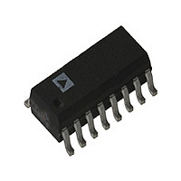
AD8803AR-REEL Analog Devices Inc, AD8803AR-REEL Datasheet - Page 2

AD8803AR-REEL
Manufacturer Part Number
AD8803AR-REEL
Description
Manufacturer
Analog Devices Inc
Datasheet
1.AD8803AR-REEL.pdf
(16 pages)
Specifications of AD8803AR-REEL
Number Of Channels
8
Resolution
8b
Conversion Rate
1.7MSPS
Interface Type
Serial (3-Wire/SPI)
Single Supply Voltage (typ)
3/5V
Dual Supply Voltage (typ)
Not RequiredV
Settling Time
0.6us
Architecture
R-2R
Power Supply Requirement
Single
Output Type
Voltage
Integral Nonlinearity Error
±1.5LSB
Single Supply Voltage (min)
2.7V
Single Supply Voltage (max)
5.5V
Dual Supply Voltage (min)
Not RequiredV
Dual Supply Voltage (max)
Not RequiredV
Operating Temp Range
-40C to 85C
Operating Temperature Classification
Industrial
Mounting
Surface Mount
Pin Count
16
Package Type
SOIC N
Lead Free Status / Rohs Status
Not Compliant
AD8801/AD8803–SPECIFICATIONS
Parameter
STATIC ACCURACY
Specifications Apply to All DACs
REFERENCE INPUT
DIGITAL INPUTS
POWER SUPPLIES
DYNAMIC PERFORMANCE
SWITCHING CHARACTERISTICS
NOTES
1
2
3
4
5
6
Specifications subject to change without notice.
Typical values represent average readings measured at +25 C.
V
Guaranteed by design and not subject to production test.
Digital Input voltages V
Measured at a V
See timing diagram for location of measured values. All input control voltages are specified with t
level of 1.6 V.
REFH
Resolution
Integral Nonlinearity Error
Differential Nonlinearity
Full-Scale Error
Zero-Code Error
DAC Output Resistance
Output Resistance Match
Voltage Range
Input Resistance
Reference Input Capacitance
Logic High
Logic Low
Logic High
Logic Low
Input Current
Input Capacitance
Power Supply Range
Supply Current (CMOS)
Supply Current (TTL)
Shutdown Current
Power Dissipation
Power Supply Sensitivity
Power Supply Sensitivity
V
Crosstalk
Input Clock Pulse Width
Data Setup Time
Data Hold Time
CS Setup Time
CS High Pulse Width
Reset Pulse Width
CLK Rise to CS Rise Hold Time
CS Rise to Next Rising Clock
OUT
can be any value between GND and V
Settling Time (Positive or Negative)
OUT
2
pin where an adjacent V
3
4
IN
= 0 V or V
3
3
DD
for CMOS condition. DAC outputs unloaded. P
3, 6
DD
OUT
, for the AD8803 V
pin is making a full-scale voltage change.
Symbol
N
INL
DNL
G
V
R
V
V
R
C
C
V
V
V
V
I
C
V
I
I
I
P
PSRR
PSRR
t
CT
t
t
t
t
t
t
t
t
IL
DD
DD
REFH
S
CH
DS
DH
CSS
CSW
RS
CSH
CS1
R/R
DISS
ZSE
OUT
REFH
REFL
REFH
IH
IL
IH
IL
DD
FSE
REF0
REF1
IL
, t
Range
O
CL
REFL
Conditions
Guaranteed Monotonic
Pin Available on AD8803 Only
Digital Inputs = 55
Digital Inputs All Zeros
Digital Inputs All Ones
V
V
V
V
V
V
V
SHDN = 0
V
V
V
See Note 5, f = 100 kHz
Clock Level High or Low
can be any value between GND and V
DD
DD
DD
DD
IN
IH
IH
IH
DD
DD
1/2 LSB Error Band
= 0 V or +5 V
= V
= 2.4 V or V
= V
= +5 V
= +5 V
= +3 V
= +3 V
= 5 V
= 3 V
DD
DD
–2–
or V
or V
(V
10%, V
10%, V
DD
T
IL
IL
A
DISS
IL
= +3 V
= 0 V
= 0 V, V
= 0.8 V, V
H
+85 C unless otherwise noted)
is calculated from (I
, V
REFH
REFH
R
REFH
= t
= +4.5 V
= +2.7 V
DD
F
10% or +5 V
= 2 ns (10% to 90% of V
= V
DD
= +5.5 V
= +5.5 V
DD
DD
.
DD
V
DD
10%, V
Min
8
–1.5
–1
–4
–0.5
3
0
0
2.4
2.1
2.7
15
5
5
10
10
60
15
10
).
DD
REFH
) and timed from a voltage
= +V
–2.8
5
1
2
25
25
5
0.01
1
0.01
0.001
0.6
50
Typ
0.01
1/2
1/4
0.1
1
DD
, V
Max
+1.5
+1
+0.5
+0.5
8
V
V
0.8
0.6
5.5
5
4
5
27.5
0.002
REFL
1
DD
DD
= 0 V, –40 C
REV. A
Units
Bits
LSB
LSB
LSB
LSB
k
%
V
V
k
pF
pF
V
V
V
V
pF
V
mA
%/%
%/%
dB
ns
ns
ns
ns
ns
ns
ns
ns
A
A
A
W
s


