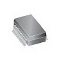
ICS8735AM-21 IDT, Integrated Device Technology Inc, ICS8735AM-21 Datasheet - Page 10

ICS8735AM-21
Manufacturer Part Number
ICS8735AM-21
Description
Manufacturer
IDT, Integrated Device Technology Inc
Type
Zero Delay PLL Clock Generatorr
Datasheet
1.ICS8735AM-21.pdf
(20 pages)
Specifications of ICS8735AM-21
Number Of Elements
1
Supply Current
150mA
Pll Input Freq (min)
31.25MHz
Pll Input Freq (max)
700MHz
Operating Supply Voltage (typ)
3.3V
Operating Temp Range
0C to 70C
Package Type
SOIC
Output Frequency Range
Up to 700MHz
Operating Supply Voltage (min)
3.135V
Operating Supply Voltage (max)
3.465V
Operating Temperature Classification
Commercial
Pin Count
20
Lead Free Status / Rohs Status
Not Compliant
Available stocks
Company
Part Number
Manufacturer
Quantity
Price
Company:
Part Number:
ICS8735AM-21LF
Manufacturer:
IDT
Quantity:
165
Company:
Part Number:
ICS8735AM-21LFT
Manufacturer:
XILINX
Quantity:
491
Power Supply Filtering Technique
As in any high speed analog circuitry, the power supply pins are
vulnerable to random noise. To achieve optimum jitter perform-
ance, power supply isolation is required. The ICS8735-21 provides
separate power supplies to isolate any high switching noise from
the outputs to the internal PLL. V
individually connected to the power supply plane through vias, and
0.01µF bypass capacitors should be used for each pin. Figure 1
illustrates this for a generic V
requires that an additional 10Ω resistor along with a 10µF bypass
capacitor be connected to the V
be replaced by a ferrite bead.
Wiring the Differential Input to Accept Single Ended Levels
Figure 2 shows how the differential input can be wired to accept
single ended levels. The reference voltage V_REF = V
generated by the bias resistors R1, R2 and C1. This bias circuit
should be located as close as possible to the input pin. The ratio of
R1 and R2 might need to be adjusted to position the V_REF in the
center of the input voltage swing. For example, if the input clock
swing is only 2.5V and V
R2/R1 = 0.609.
IDT™ / ICS™ 3.3V LVPECL ZERO DELAY CLOCK GENERATOR
ICS8735-21
700MHZ, DIFFERENTIAL-TO-3.3V LVPECL ZERO DELAY CLOCK GENERATOR
CC
= 3.3V, V_REF should be 1.25V and
CC
CCA
pin and also shows that V
CC,
pin. The 10Ω resistor can also
V
CCA
and V
CCO
should be
CC
/2 is
CCA
10
Figure 2. Single-Ended Signal Driving Differential Input
Single Ended Clock Input
Figure 1. Power Supply Filtering
C1
0.1u
V_REF
V
V
CCA
CC
ICS8735AM-21 REV. A JULY 31, 2008
.01µF
.01µF
R1
1K
R2
1K
3.3V
V
CC
10Ω
10µF
CLK
nCLK


