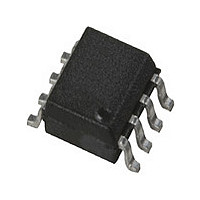
HMMC-3122-TR1 Avago Technologies US Inc., HMMC-3122-TR1 Datasheet - Page 4

HMMC-3122-TR1
Manufacturer Part Number
HMMC-3122-TR1
Description
Manufacturer
Avago Technologies US Inc.
Datasheet
1.HMMC-3122-TR1.pdf
(8 pages)
Specifications of HMMC-3122-TR1
Pin Count
8
Screening Level
Industrial
Package Type
SOIC
Lead Free Status / Rohs Status
Compliant
Applications
The HMMC-3122 is designed for use in high frequency
communications, microwave instrumentation, and EW
radar systems where low phase–noise PLL control
circuitry or broad–band frequency translation is
required.
Operation
The device is designed to operate when driven with
either a single–ended or differential sinusoidal input
signal over a 200 MHz to 12 GHz bandwidth. Below
200 MHz the prescaler input is “slew–rate” limited,
requiring fast rising and falling edge speeds to properly
divide. The device will operate at frequencies down to
dc when driven with a square–wave.
Due to the presence of an off– chip RF–bypass
capacitor inside the package (connected to the V
contact on the device), and the unique design of the
device itself, the component may be biased from either
a single positive or single negative supply bias. The
backside of the package is not dc connected to any dc
bias point on the device.
For positive supply operation, V
biased at any voltage in the +4.5 to +6.5 volt range
with pin 8 (V
V
between -4.5 to -6.5 volts is applied to pin 8 (V
Figure 1. Simplified Schematic
IN
IN
4
CC
pins are typically grounded and a negative voltage
5
7
SOIC8 w/Backside GND
EE
By
poss
) grounded. For negative bias operation
IN
IN
50
V
6
V cc
CC
50
150p
CC
pins are nominally
V
4
V cc
V
8
V ee
CC
÷
EE
EE
).
CC
50
V
2
V cc
CC
Vpwr
sel
ac–Coupling and dc–Blocking
All RF ports are dc connected on–chip to the V
contact through on–chip 50Ω resistors. Under any bias
conditions where V
should be ac coupled via series capacitors mounted
on the PC– board at each RF port. Only under bias
conditions where V
negative bias supply operation) may the RF ports be
direct coupled to adjacent circuitry or in some cases,
such as level shifting to subsequent stages. In the latter
case the package heat sink may be “floated” and bias
applied as the difference between V
Input dc Offset
If an RF signal with sufficient signal to noise ratio is
present at the RF input lead, the prescaler will operate
and provide a divided output equal the input frequency
divided by the divide modulus. Under certain “ideal”
conditions where the input is well matched at the right
input frequency, the component may “self–oscillate”,
especially under small signal input powers or with only
noise present at the input. This “self–oscillation” will
produce an undesired output signal also known as a
false trigger. To prevent false triggers or self– oscillation
conditions, apply a 20 to 100 mV dc offset voltage
between the RFin and RFin ports. This prevents noise
or spurious low level signals from triggering the divider.
Adding a 10KΩ resistor between the unused RF input
to a contact point at the VEE potential will result in an
offset of » 25mV between the RF inputs. Note, however,
that the input sensitivity will be reduced slightly due
to the presence of this offset.
50
OUT
OUT
3
Pin 1
OUT
OUT
CC
CC
is not dc grounded the RF ports
is dc grounded (as is typical for
CC
and V
EE
.
CC


