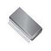
TDA5251XT Infineon Technologies, TDA5251XT Datasheet - Page 8

TDA5251XT
Manufacturer Part Number
TDA5251XT
Description
Manufacturer
Infineon Technologies
Datasheet
1.TDA5251XT.pdf
(88 pages)
Specifications of TDA5251XT
Operating Temperature (min)
-40C
Operating Temperature (max)
85C
Operating Temperature Classification
Industrial
Product Depth (mm)
4.4mm
Product Length (mm)
9.7mm
Operating Supply Voltage (min)
2.1V
Operating Supply Voltage (max)
5.5V
Lead Free Status / Rohs Status
Compliant
1
1.1
The IC is a low power consumption single chip FSK/ASK Transceiver for the frequency band
315MHz. The IC combines a very high level of integration and minimum external part count. The
device contains a low noise amplifier (LNA), a double balanced mixer, a fully integrated VCO, a PLL
synthesizer, a crystal oscillator with FSK modulator, a limiter with RSSI generator, an FSK
demodulator, a data filter, a data comparator (slicer), a positive and a negative data peak detector,
a highly efficient power amplifier and a complex digital timing and control unit with I
microcontroller interface. Additionally there is a power down feature to save battery power.
The transmit section uses direct ASK modulation by switching the power amplifier, and crystal
oscillator detuning for FSK modulation. The necessary detuning load capacitors are external. The
capacitors for fine tuning are integrated. The receive section is using a novel single-conversion/
direct-conversion scheme that is combining the advantages of both receive topologies. The IF is
contained on the chip, no RF channel filters are necessary as the channel filter is also on the chip.
The self-polling logic can be used to let the device operate autonomously as a master for a decoding
microcontroller.
1.2
– Low supply current (I
– Supply voltage range 2.1 V to 5.5 V
– Operating temperature range -40°C to +85°C
– Power down mode with very low supply current consumption
– FSK and ASK modulation and demodulation capability without external circuitry changes, FM
– Fully integrated VCO and PLL synthesizer and loop filter on-chip with on-chip crystal oscillator
– Differential receive signal path completely on-chip, therefore no external filters are necessary
– On-chip low pass channel select and data filter with tuneable bandwith
– Data slicer with self-adjusting threshold and 2 peak detectors
– Self-polling logic with adjustable duty cycle and ultrafast data rate detection and timer mode
– FSK and ASK sensitivity < -109 dBm
– Adjustable LNA gain
– Digital RSSI and Battery Voltage Readout
– Provides Clock Out Pin for external microcontroller
– Transmit power up to +13 dBm in 50Ω load at 5V supply voltage
– I
Data Sheet
voltage, 25°C)
demodulation capability
tuning, therefore no additional external components necessary
providing periodical interrupt
2
C/3-wire microcontroller interface, working at max. 400kbit/s
Product Description
Overview
Features
s
= 9 mA typ. receive, I
s
8
= 13mA typ. transmit mode, both at 3 V supply
Product Description
TDA5251 F1
Version 1.1
2007-02-26
2
C/3-wire


