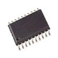
T5760NTGS Atmel, T5760NTGS Datasheet - Page 5

T5760NTGS
Manufacturer Part Number
T5760NTGS
Description
Manufacturer
Atmel
Datasheet
1.T5760NTGS.pdf
(38 pages)
Specifications of T5760NTGS
Operating Temperature (min)
-40C
Operating Temperature (max)
105C
Operating Temperature Classification
Industrial
Lead Free Status / Rohs Status
Not Compliant
4. Analog Signal Processing
4.1
4.2
4561C–RKE–05/05
IF Filter
Limiting RSSI Amplifier
To determine f
frequency is f
is tuned by the crystal frequency f
f
f
The relation is designed to achieve the nominal IF frequency of f
version. For the 915 MHz version an IF frequency of f
The RF input either from an antenna or from an RF generator must be transformed to the RF
input pin LNA_IN. The input impedance of that pin is provided in the electrical parameters. The
parasitic board inductances and capacitances influence the input matching. The RF receiver
T5760/T5761 exhibits its highest sensitivity if the LNA is power matched. This makes the match-
ing to an SAW filter as well as to 50 or an antenna easier.
Figure 14-1 on page 29
ure 14-2 on page 29
matching network shown in
given in the electrical characteristics.
The signals coming from the RF front-end are filtered by the fully integrated 4th-order IF filter.
The IF center frequency is f
f
The subsequent RSSI amplifier enhances the output signal of the IF amplifier before it is fed into
the demodulator. The dynamic range of this amplifier is R
operated within its linear range, the best S/N ratio is maintained in ASK mode. If the dynamic
range is exceeded by the transmitter signal, the S/N ratio is defined by the ratio of the maximum
RSSI output voltage and the RSSI output voltage due to a disturber. The dynamic range of the
RSSI amplifier is exceeded if the RF input signal is about 60 dB higher compared to the RF input
signal at full sensitivity.
In FSK mode the S/N ratio is not affected by the dynamic range of the RSSI amplifier, because
only the hard limited signal from a high gain limiting amplifier is used by the demodulator.
The output voltage of the RSSI amplifier is internally compared to a threshold voltage V
V
SENS and GND or V
means it is possible to operate the receiver at a lower sensitivity.
If R
nect the pin SENS directly to GND to get the maximum sensitivity.
If R
defined by the value of R
input. The reduced sensitivity depends on the signal strength at the output of the RSSI amplifier.
LO
IF
IF
Th_red
.
= f
= 1.0 MHz for f
Sens
Sens
LO
is determined by the value of the external resistor R
/915
is connected to V
is connected to GND, the receiver switches to full sensitivity. It is also possible to con-
IF
LO
= 950 kHz. To achieve a good accuracy of the filter corner frequencies, the filter
, the construction of the IF filter must be considered at this point. The nominal IF
RF
= 915 MHz. The nominal bandwidth is 600 kHz.
illustrates an according input matching for 868.3 MHz to an SAW. The input
S
. The output of the comparator is fed into the digital control logic. By this
shows a typical input matching network for f
S
, the receiver operates at a lower sensitivity. The reduced sensitivity is
Sens
Figure 14-1 on page 29
, the maximum sensitivity by the signal-to-noise ratio of the LNA
IF
XTO
= 950 kHz for applications where f
. This means that there is a fixed relation between f
is the reference network for the parameters
IF
= 1.0 MHz results.
Sens
RSSI
. R
= 60 dB. If the RSSI amplifier is
IF
Sens
= 950 kHz for the 868.3 MHz
RF
is connected between pin
= 868.3 MHz to 50 .
T5760/T5761
RF
= 868.3 MHz and
IF
Th_red
and
Fig-
5
.


