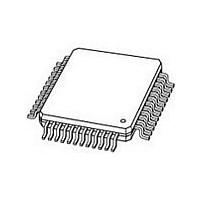
"CX24109-11Z,518" NXP Semiconductors, "CX24109-11Z,518" Datasheet - Page 16

"CX24109-11Z,518"
Manufacturer Part Number
"CX24109-11Z,518"
Description
Manufacturer
NXP Semiconductors
Datasheet
1.CX24109-11Z518.pdf
(40 pages)
Specifications of "CX24109-11Z,518"
Lead Free Status / Rohs Status
Compliant
- Current page: 16 of 40
- Download datasheet (250Kb)
NXP Semiconductors
Figure 4.
Figure 5.
Table 3.
CX24109_N_1
Product data sheet
MSB
20
MSB
0
0
1
d20 d19
Control
Bits
19
0
1
0
Enable
Clock
Data
Programming Bit Mapping (Sheet 1 of 2)
Serial Interface Programming Example
Programming Word Configuration
18
R
R
R
d18 d17 d16 d15 d14 d13 d12 d11
17
R
16
R
The internal shift register in the CX24109 is 21 bits long. When the data is latched into the IC,
the two MSBs act as control bits, and the lower 19 bits are the data bits as illustrated in
Figure
The control bits determine the functional block that is being programmed, while the data bits
contain the specific control information.
data bits.
15
R
5. Data must be entered MSB first.
14
R
VGA2 Offset
VCA Offset
13
R
Rev. 01 — 13 November 2008
12
Programming Bit Mapping
R
VGA Programming
VCA Programming
PLL Programming
R
11
(1)
Band Select
d10
Data Bits
. . .
. . .
10
R
d9
9
V
Table 3
d8
R
8
(1)
d7
provides a detail mapping of the control and
7
d6
Chapter 1: Functional Description
6
d5
d4
5
VGA1 Offset
VCA Slope
d3
Band Select
4
d2
3
CX24109
© NXP B.V. 2008. All rights reserved.
d1
2
LSB
102031_005
102031_006
d0
1
LSB
0
16
Related parts for "CX24109-11Z,518"
Image
Part Number
Description
Manufacturer
Datasheet
Request
R
Part Number:
Description:
Manufacturer:
NXP Semiconductors
Datasheet:
Part Number:
Description:
Manufacturer:
NXP Semiconductors
Datasheet:

Part Number:
Description:
IC SATELLITE TUNER DGTL 48-ETQFP
Manufacturer:
NXP Semiconductors
Datasheet:

Part Number:
Description:
IC SATELLITE TUNER DGTL 48-ETQFP
Manufacturer:
NXP Semiconductors
Datasheet:
Part Number:
Description:
NXP Semiconductors designed the LPC2420/2460 microcontroller around a 16-bit/32-bitARM7TDMI-S CPU core with real-time debug interfaces that include both JTAG andembedded trace
Manufacturer:
NXP Semiconductors
Datasheet:

Part Number:
Description:
NXP Semiconductors designed the LPC2458 microcontroller around a 16-bit/32-bitARM7TDMI-S CPU core with real-time debug interfaces that include both JTAG andembedded trace
Manufacturer:
NXP Semiconductors
Datasheet:
Part Number:
Description:
NXP Semiconductors designed the LPC2468 microcontroller around a 16-bit/32-bitARM7TDMI-S CPU core with real-time debug interfaces that include both JTAG andembedded trace
Manufacturer:
NXP Semiconductors
Datasheet:
Part Number:
Description:
NXP Semiconductors designed the LPC2470 microcontroller, powered by theARM7TDMI-S core, to be a highly integrated microcontroller for a wide range ofapplications that require advanced communications and high quality graphic displays
Manufacturer:
NXP Semiconductors
Datasheet:
Part Number:
Description:
NXP Semiconductors designed the LPC2478 microcontroller, powered by theARM7TDMI-S core, to be a highly integrated microcontroller for a wide range ofapplications that require advanced communications and high quality graphic displays
Manufacturer:
NXP Semiconductors
Datasheet:
Part Number:
Description:
The Philips Semiconductors XA (eXtended Architecture) family of 16-bit single-chip microcontrollers is powerful enough to easily handle the requirements of high performance embedded applications, yet inexpensive enough to compete in the market for hi
Manufacturer:
NXP Semiconductors
Datasheet:
Part Number:
Description:
The XA-S3 device is a member of Philips Semiconductors? XA(eXtended Architecture) family of high performance 16-bitsingle-chip microcontrollers
Manufacturer:
NXP Semiconductors
Datasheet:

Part Number:
Description:
The NXP BlueStreak LH75401/LH75411 family consists of two low-cost 16/32-bit System-on-Chip (SoC) devices
Manufacturer:
NXP Semiconductors
Datasheet:

Part Number:
Description:
The NXP LPC3130/3131 combine an 180 MHz ARM926EJ-S CPU core, high-speed USB2
Manufacturer:
NXP Semiconductors
Datasheet:


