74ABT823DB NXP Semiconductors, 74ABT823DB Datasheet
74ABT823DB
Specifications of 74ABT823DB
Available stocks


Related parts for 74ABT823DB


74ABT823DB Summary of contents
Page 1
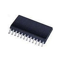
... Table 1. Ordering information Type number Package Temperature range Name −40 °C to +85 °C 74ABT823D −40 °C to +85 °C 74ABT823DB −40 °C to +85 °C 74ABT823PW Description SO24 plastic small outline package; 24 leads; body width 7.5 mm SSOP24 plastic shrink small outline package; 24 leads; ...
Page 2
... NXP Semiconductors 4. Functional diagram Fig 1. Logic symbol 74ABT823_3 Product data sheet 9-bit D-type flip-flop with reset and enable; 3-state 001aaa847 Fig 2. IEC logic symbol All information provided in this document is subject to legal disclaimers. Rev. 03 — 23 March 2010 74ABT823 1C2 001aaa848 © NXP B.V. 2010. All rights reserved. ...
Page 3
... NXP Semiconductors Fig 3. Logic diagram 74ABT823_3 Product data sheet 9-bit D-type flip-flop with reset and enable; 3-state FF0 FF1 FF5 FF6 Q5 Q6 All information provided in this document is subject to legal disclaimers. Rev. 03 — 23 March 2010 74ABT823 FF2 FF3 FF4 FF7 FF8 Q7 Q8 001aac444 © ...
Page 4
... NXP Semiconductors 5. Pinning information 5.1 Pinning Fig 4. Pin configuration 5.2 Pin description Table 2. Pin description Symbol OE D0, D1, D2, D3, D4, D5, D6, D7 GND CP CE Q8, Q7, Q6, Q5, Q4, Q3, Q3, Q2, Q1, Q0 15, 16, 17, 18, 19, 20, 21, 22 74ABT823_3 Product data sheet 9-bit D-type flip-flop with reset and enable; 3-state ...
Page 5
... NXP Semiconductors 6. Functional description 6.1 Function table [1] Table 3. Function table Input [ HIGH voltage level LOW voltage level HIGH voltage level one set-up time prior to the LOW-to-HIGH clock transition LOW voltage level one set-up time prior to the LOW-to-HIGH clock transition; ↑ = LOW-to-HIGH clock transition; ...
Page 6
... NXP Semiconductors 8. Recommended operating conditions Table 5. Operating conditions Voltages are referenced to GND (ground = 0 V). Symbol Parameter V supply voltage CC V input voltage I V HIGH-level input voltage IH V LOW-level Input voltage IL I HIGH-level output current OH I LOW-level output current OL Δt/ΔV input transition rise and fall rate ...
Page 7
... NXP Semiconductors Table 6. Static characteristics Symbol Parameter ΔI additional supply CC current C input capacitance I C output capacitance O [1] For valid test results, data must not be loaded into the flip-flops (or latches) after applying the power. [2] This parameter is valid for any V a transition time 100 μs is permitted. ...
Page 8
... NXP Semiconductors Table 7. Dynamic characteristics GND = 0 V; for test circuit, see Figure Symbol Parameter Conditions t pulse width LOW CP; see WL MR; see t recovery time MR to CP; see rec 11. Waveforms CP input Qn output and V are typical voltage output levels that occur with the output load. ...
Page 9
... NXP Semiconductors CP input Dn, CE input The shaded areas indicate when the input is permitted to change for predictable output performance. Fig 7. Set-up and hold times data output (Dn) to clock (CP) and clock enable input (CE) to clock (CP) OE input Qn output Qn output and V are typical voltage output levels that occur with the output load ...
Page 10
... NXP Semiconductors negative V M pulse positive V M pulse Input pulse definition Test data is given in Table R = Load resistance Load capacitance including jig and probe capacitance Termination resistance should be equal to output impedance External voltage for measuring switching times. EXT Fig 9. Load circuitry for switching times Table 8 ...
Page 11
... NXP Semiconductors 12. Package outline SO24: plastic small outline package; 24 leads; body width 7 pin 1 index 1 e DIMENSIONS (inch dimensions are derived from the original mm dimensions) A UNIT max. 0.3 2.45 mm 2.65 0.25 0.1 2.25 0.012 0.096 inches 0.1 0.01 0.004 0.089 Note 1. Plastic or metal protrusions of 0.15 mm (0.006 inch) maximum per side are not included. ...
Page 12
... NXP Semiconductors SSOP24: plastic shrink small outline package; 24 leads; body width 5 pin 1 index 1 DIMENSIONS (mm are the original dimensions) A UNIT max. 0.21 1. 0.25 0.05 1.65 Note 1. Plastic or metal protrusions of 0.2 mm maximum per side are not included. OUTLINE VERSION IEC SOT340-1 Fig 11. Package outline SOT340-1 (SSOP24) ...
Page 13
... NXP Semiconductors TSSOP24: plastic thin shrink small outline package; 24 leads; body width 4 pin 1 index 1 DIMENSIONS (mm are the original dimensions) A UNIT max. 0.15 0.95 mm 1.1 0.25 0.05 0.80 Notes 1. Plastic or metal protrusions of 0.15 mm maximum per side are not included. 2. Plastic interlead protrusions of 0.25 mm maximum per side are not included. ...
Page 14
... Modifications: The format of this data sheet has been redesigned to comply with the new identity guidelines of NXP Semiconductors. • Legal texts have been adapted to the new company name where appropriate. • DIP 24 (SOT222-1) package removed from 12 “Package outline” ...
Page 15
... In no event shall NXP Semiconductors be liable for any indirect, incidental, punitive, special or consequential damages (including - without limitation - lost profits, lost savings, business interruption, costs related to the removal or ...
Page 16
... NXP Semiconductors 16. Contact information For more information, please visit: For sales office addresses, please send an email to: 74ABT823_3 Product data sheet 9-bit D-type flip-flop with reset and enable; 3-state http://www.nxp.com salesaddresses@nxp.com All information provided in this document is subject to legal disclaimers. Rev. 03 — 23 March 2010 74ABT823 © ...
Page 17
... NXP Semiconductors 17. Contents 1 General description . . . . . . . . . . . . . . . . . . . . . . 1 2 Features and benefits . . . . . . . . . . . . . . . . . . . . 1 3 Ordering information . . . . . . . . . . . . . . . . . . . . . 1 4 Functional diagram . . . . . . . . . . . . . . . . . . . . . . 2 5 Pinning information . . . . . . . . . . . . . . . . . . . . . . 4 5.1 Pinning . . . . . . . . . . . . . . . . . . . . . . . . . . . . . . . 4 5.2 Pin description . . . . . . . . . . . . . . . . . . . . . . . . . 4 6 Functional description . . . . . . . . . . . . . . . . . . . 5 6.1 Function table . . . . . . . . . . . . . . . . . . . . . . . . . . 5 7 Limiting values Recommended operating conditions Static characteristics Dynamic characteristics . . . . . . . . . . . . . . . . . . 7 11 Waveforms . . . . . . . . . . . . . . . . . . . . . . . . . . . . . 8 12 Package outline ...