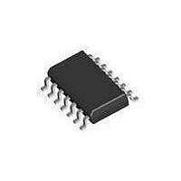
74HC00D NXP Semiconductors, 74HC00D Datasheet - Page 3

74HC00D
Manufacturer Part Number
74HC00D
Description
Gates (AND / NAND / OR / NOR) QUAD 2-IN NAND GATE
Manufacturer
NXP Semiconductors
Datasheet
1.74HCT00PW118.pdf
(16 pages)
Specifications of 74HC00D
Product
NAND
Logic Family
74HC
Number Of Gates
Quad
Number Of Lines (input / Output)
8 / 4
High Level Output Current
- 5.2 mA
Low Level Output Current
5.2 mA
Propagation Delay Time
7 ns
Supply Voltage (max)
6 V
Supply Voltage (min)
2 V
Maximum Operating Temperature
+ 125 C
Mounting Style
SMD/SMT
Package / Case
SOT-108
Minimum Operating Temperature
- 40 C
Lead Free Status / Rohs Status
Details
Other names
74HC00D,652
Available stocks
Company
Part Number
Manufacturer
Quantity
Price
Part Number:
74HC00D
Manufacturer:
PH
Quantity:
20 000
Part Number:
74HC00D,652
Manufacturer:
NEXPERIA/安世
Quantity:
20 000
Company:
Part Number:
74HC00D,653
Manufacturer:
GGM
Quantity:
70
Company:
Part Number:
74HC00DT
Manufacturer:
samwha
Quantity:
73 715
Company:
Part Number:
74HC00DTR2G
Manufacturer:
ON Semiconductor
Quantity:
800
NXP Semiconductors
Table 2.
6. Functional description
Table 3.
[1]
7. Limiting values
Table 4.
In accordance with the Absolute Maximum Rating System (IEC 60134). Voltages are referenced to GND (ground = 0 V).
[1]
[2]
74HC_HCT00
Product data sheet
Symbol
1Y to 4Y
GND
V
Input
nA
L
X
H
Symbol
V
I
I
I
I
I
T
P
IK
OK
O
CC
GND
stg
CC
CC
tot
H = HIGH voltage level; L = LOW voltage level; X = don’t care.
The input and output voltage ratings may be exceeded if the input and output current ratings are observed.
For DIP14 package: P
For SO14 package: P
For (T)SSOP14 packages: P
For DHVQFN14 packages: P
Pin description
Function table
Limiting values
Parameter
supply voltage
input clamping current
output clamping current
output current
supply current
ground current
storage temperature
total power dissipation
DIP14 package
SO14, (T)SSOP14 and
DHVQFN14 packages
Pin
3, 6, 8, 11
7
14
tot
tot
derates linearly with 8 mW/K above 70 C.
derates linearly with 12 mW/K above 70 C.
[1]
…continued
tot
tot
derates linearly with 5.5 mW/K above 60 C.
derates linearly with 4.5 mW/K above 60 C.
Description
data output
ground (0 V)
supply voltage
nB
X
L
H
All information provided in this document is subject to legal disclaimers.
Rev. 5 — 25 November 2010
Conditions
V
V
0.5 V < V
I
O
< 0.5 V or V
< 0.5 V or V
O
< V
I
CC
O
> V
> V
+ 0.5 V
CC
CC
+ 0.5 V
+ 0.5 V
74HC00; 74HCT00
Output
nY
H
H
L
[1]
[1]
[2]
Quad 2-input NAND gate
Min
0.5
-
-
-
-
50
65
-
-
© NXP B.V. 2010. All rights reserved.
Max
+7
20
20
25
50
-
+150
750
500
Unit
V
mA
mA
mA
mA
mA
C
mW
mW
3 of 16


