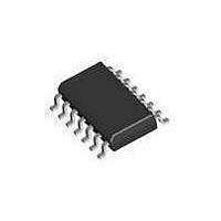
N74F74D NXP Semiconductors, N74F74D Datasheet - Page 2

N74F74D
Manufacturer Part Number
N74F74D
Description
Flip Flops DUAL D F/F EDGE TRIG
Manufacturer
NXP Semiconductors
Datasheet
1.N74F74N602.pdf
(8 pages)
Specifications of N74F74D
Number Of Circuits
2
Logic Family
N74F
Logic Type
D-Type Flip-Flop
Polarity
Inverting/Non-Inverting
Input Type
Single-Ended
Propagation Delay Time
8.5 ns
High Level Output Current
- 1 mA
Supply Voltage (max)
5.5 V
Maximum Operating Temperature
+ 85 C
Mounting Style
SMD/SMT
Package / Case
SOT-108
Minimum Operating Temperature
- 40 C
Supply Voltage (min)
4.5 V
Lead Free Status / Rohs Status
Details
Other names
N74F74D,602
Available stocks
Company
Part Number
Manufacturer
Quantity
Price
Company:
Part Number:
N74F74D
Manufacturer:
PHILIPS
Quantity:
1 376
Part Number:
N74F74D
Manufacturer:
PHILIPS/飞利浦
Quantity:
20 000
Philips Semiconductors
FEATURE
DESCRIPTION
The 74F74 is a dual positive edge-triggered D-type flip-flop featuring
individual data, clock, set, and reset inputs; also true and
complementary outputs. Set (SD) and reset (RD) are asynchronous
active low inputs and operate independently of the clock input. When
set and reset are inactive (high), data at the D input is transferred to
the Q and Q outputs on the low-to-high transition of the clock. Data
must be stable just one setup time prior to the low-to-high transition of
the clock for predictable operation. Clock triggering occurs at a
voltage level and is not directly related to the transition time of the
positive-going pulse. Following the hold time interval, data at the D
input may be changed without affecting the levels of the output.
ORDERING INFORMATION
INPUT AND OUTPUT LOADING AND FAN OUT TABLE
NOTE: One (1.0) FAST unit load is defined as: 20 A in the high state and 0.6mA in the low state.
LOGIC SYMBOL
1996 Mar 12
V
GND = Pin 7
Industrial temperature range available (–40 C to +85 C)
Dual D-type flip-flop
74F74
CC
Q0, Q1, Q0, Q1
= Pin 14
RD0, RD1
CP0, CP1
SD0, SD1
14-pin plastic DIP
14-pin plastic SO
D0, D1
DESCRIPTION
PINS
TYPE
10
13
11
3
4
1
CP0
SD0
RD0
CP1
SD1
RD1
Data inputs
Clock inputs (active rising edge)
Set inputs (active low)
Reset inputs (active low)
Data outputs
Q0 Q0 Q1 Q1
5
D0 D1
6
2
12
9
SF00046
8
COMMERCIAL RANGE
DESCRIPTION
T
amb
TYPICAL f
V
CC
125MHz
= 0 C to +70 C
N74F74N
N74F74D
= 5V 10%,
max
ORDER CODE
2
PIN CONFIGURATION
IEC/IEEE SYMBOL
74F (U.L.) HIGH/LOW
T
INDUSTRIAL RANGE
amb
V
CC
= –40 C to +85 C
1.0/1.0
1.0/1.0
1.0/3.0
1.0/3.0
50/33
I74F74N
I74F74D
= 5V 10%,
12
13
10
11
TYPICAL SUPPLY CURRENT (TOTAL)
4
3
2
1
GND
RD0
CP0
SD0
D0
Q0
Q0
1
2
3
4
5
6
7
1D
R
S
S
2D
R
C1
C2
11.5mA
&
LOAD VALUE HIGH/LOW
SF00045
14
13
12
11
10
9
8
V
RD1
D1
CP1
SD1
Q1
Q1
1.0mA/20mA
CC
20 A/0.6mA
20 A/0.6mA
20 A/1.8mA
20 A/1.8mA
SF00047
Product specification
PKG. DWG. #
SOT108-1
SOT27-1
5
6
9
8
853 0335 16554
74F74


