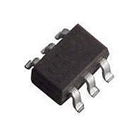
74LVC2G17GW-G NXP Semiconductors, 74LVC2G17GW-G Datasheet - Page 8

74LVC2G17GW-G
Manufacturer Part Number
74LVC2G17GW-G
Description
Buffers & Line Drivers 3.3V DUAL SCHMITT TRIGGER BUFF
Manufacturer
NXP Semiconductors
Datasheet
1.74LVC2G17GV125.pdf
(19 pages)
Specifications of 74LVC2G17GW-G
Logic Family
LVC
Logic Type
CMOS
Number Of Channels Per Chip
2
Polarity
Non-Inverting
Supply Voltage (max)
5.5 V
Supply Voltage (min)
1.65 V
Maximum Operating Temperature
+ 125 C
Mounting Style
SMD/SMT
Package / Case
SOT-363-6
High Level Output Current
- 32 mA
Low Level Output Current
32 mA
Minimum Operating Temperature
- 40 C
Number Of Lines (input / Output)
2 / 2
Propagation Delay Time
3.8 ns at 2.7 V
Lead Free Status / Rohs Status
Details
Other names
74LVC2G17GW,125
NXP Semiconductors
14. Transfer characteristics
Table 11.
At recommended operating conditions. Voltages are referenced to GND (ground = 0 V).
[1]
15. Waveforms transfer characteristics
74LVC2G17
Product data sheet
Symbol Parameter
V
V
V
Fig 9.
T+
T−
H
All typical values are measured at T
positive-going
threshold voltage
negative-going
threshold voltage
hysteresis voltage (V
Transfer characteristic
Transfer characteristics
V
O
V
T−
V
H
Conditions
see
see
Figure 10
V
V
V
V
V
V
V
V
V
V
V
T+
V
V
V
V
V
T+
CC
CC
CC
CC
CC
CC
CC
CC
CC
CC
CC
CC
CC
CC
CC
Figure 9
Figure 9
− V
amb
= 1.8 V
= 2.3 V
= 3.0 V
= 4.5 V
= 5.5 V
= 1.8 V
= 2.3 V
= 3.0 V
= 4.5 V
= 5.5 V
= 1.8 V
= 2.3 V
= 3.0 V
= 4.5 V
= 5.5 V
T−
= 25 °C.
and
); see
mnb154
All information provided in this document is subject to legal disclaimers.
and
and
V
Figure 11
I
Figure
Figure 10
Figure 10
Rev. 5 — 6 August 2010
9,
Dual non-inverting Schmitt trigger with 5 V tolerant input
Fig 10. Definition of V
0.70
1.00
1.30
1.90
2.20
0.25
0.40
0.60
1.00
1.20
0.15
0.25
0.40
0.60
0.70
Min
V
−40 °C to +85 °C
T+
V
V
O
I
and V
Typ
1.10
1.40
1.76
2.47
2.91
0.61
0.80
1.04
1.55
1.86
0.49
0.60
0.73
0.92
1.02
T−
V
[1]
T+
limits at 70 % and 20 %.
T+
Max
1.50
1.80
2.20
3.10
3.60
0.90
1.15
1.50
2.00
2.30
1.00
1.10
1.20
1.50
1.70
, V
T−
and V
V
74LVC2G17
T−
−40 °C to +125 °C Unit
0.70
1.00
1.30
1.90
2.20
0.25
0.40
0.60
1.00
1.20
0.15
0.25
0.40
0.60
0.70
Min
H
© NXP B.V. 2010. All rights reserved.
mnb155
V
Max
1.70
2.00
2.40
3.30
3.80
1.10
1.35
1.70
2.20
2.50
1.20
1.30
1.40
1.70
1.90
H
8 of 19
V
V
V
V
V
V
V
V
V
V
V
V
V
V
V


