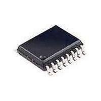
74LV4052PW NXP Semiconductors, 74LV4052PW Datasheet - Page 5

74LV4052PW
Manufacturer Part Number
74LV4052PW
Description
Multiplexer Switch ICs DUAL 4-CH MUX/DMUX
Manufacturer
NXP Semiconductors
Datasheet
1.74LV4052PW118.pdf
(16 pages)
Specifications of 74LV4052PW
Number Of Channels
2 Channel
On Resistance (max)
250 Ohms
Propagation Delay Time
25 ns, 9 ns, 6 ns, 5 ns, 4 ns, 3 ns
On Time (max)
190 ns
Off Time (max)
125 ns
Supply Voltage (max)
6 V
Supply Voltage (min)
1 V
Maximum Power Dissipation
400 mW
Maximum Operating Temperature
+ 125 C
Minimum Operating Temperature
- 40 C
Package / Case
TSSOP-16
Mounting Style
SMD/SMT
Number Of Lines (input / Output)
8 / 2
Lead Free Status / Rohs Status
Details
Other names
74LV4052PW,112
Available stocks
Company
Part Number
Manufacturer
Quantity
Price
Part Number:
74LV4052PW
Manufacturer:
NXP/恩智浦
Quantity:
20 000
Company:
Part Number:
74LV4052PW,118
Manufacturer:
NXP
Quantity:
150
Company:
Part Number:
74LV4052PWЈ¬118
Manufacturer:
NXP
Quantity:
7 500
1. Stresses beyond those listed may cause permanent damage to the device. These are stress ratings only and functional operation of the
2. The input and output voltage ratings may be exceeded if the input and output current ratings are observed.
Philips Semiconductors
ABSOLUTE MAXIMUM RATINGS
In accordance with the Absolute Maximum Rating System (IEC 134).
Voltages are referenced to GND (ground = 0 V).
NOTES:
RECOMMENDED OPERATING CONDITIONS
NOTE:
1. The LV is guaranteed to function down to V
1998 Jun 23
SYMBOL
SYMBOL
Dual 4-channel analog multiplexer/demultiplexer
device at these or any other conditions beyond those indicated under “recommended operating conditions” is not implied. Exposure to
absolute-maximum-rated conditions for extended periods may affect device reliability.
T
"I
V
P
"I
t
V
V
"I
T
amb
r
V
CC
, t
TOT
stg
CC
O
I
SK
IK
f
S
DC supply voltage
Input voltage
Output voltage
Operating ambient temperature range in free air
Input rise and fall times
DC supply voltage
DC input diode current
DC switch diode current
DC switch current
Storage temperature range
Power dissipation per package
– plastic DIL
– plastic mini-pack (SO)
– plastic shrink mini-pack (SSOP and TSSOP)
PARAMETER
PARAMETER
CC
1, 2
= 1.0V (input levels GND or V
V
V
–0.5 V < V
for temperature range: –40 to +125 C
above +70 C derate linearly with 12 mW/K
above +70 C derate linearly with 8 mW/K
above +60 C derate linearly with 5.5 mW/K
See Note 1 and Figure 5
I
S
< –0.5 or V
< –0.5 or V
V
V
V
CC
CC
CC
See DC and AC
5
characteristics
CONDITIONS
= 1.0 V to 2.0 V
= 2.0 V to 2.7 V
= 2.7 V to 6.0 V
CC
S
); DC characteristics are guaranteed from V
< V
I
S
> V
CONDITIONS
CC
> V
CC
+ 0.5 V
CC
+ 0.5 V
+ 0.5 V
MIN
–40
–40
1.0
0
0
–
–
–
TYP
3.3
–
–
–
–
–
–0.5 to +7.0
–65 to +150
RATING
CC
750
500
400
20
20
25
= 1.2V to V
MAX
+125
V
V
+85
Product specification
74LV4052
500
200
100
6.0
CC
CC
CC
UNIT
= 6.0V.
UNIT
mW
ns/V
mA
mA
mA
V
V
V
V
C
C


