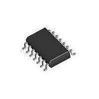
GTL2005PW NXP Semiconductors, GTL2005PW Datasheet - Page 15

GTL2005PW
Manufacturer Part Number
GTL2005PW
Description
Translation - Voltage Levels 4-BIT BI-DIREC NON-LATCH TRAN
Manufacturer
NXP Semiconductors
Datasheet
1.GTL2005PW118.pdf
(19 pages)
Specifications of GTL2005PW
Logic Type
Translator
Logic Family
GTL
Package / Case
SOT-402
Translation
GTL/GTL+ to LVTTL/TTL
High Level Output Current
- 12 mA
Low Level Output Current
40 mA
Propagation Delay Time
4.4 ns
Supply Voltage (max)
3.6 V
Supply Voltage (min)
3 V
Maximum Operating Temperature
+ 85 C
Minimum Operating Temperature
- 40 C
Mounting Style
SMD/SMT
Lead Free Status / Rohs Status
Details
Other names
GTL2005PW,112
Available stocks
Company
Part Number
Manufacturer
Quantity
Price
Company:
Part Number:
GTL2005PW
Manufacturer:
LT
Quantity:
2 380
Part Number:
GTL2005PW
Manufacturer:
PHILIPS/飞利浦
Quantity:
20 000
Part Number:
GTL2005PW,118
Manufacturer:
NXP/恩智浦
Quantity:
20 000
Part Number:
GTL2005PW-T
Manufacturer:
PHILIPS/飞利浦
Quantity:
20 000
Part Number:
GTL2005PW/DG
Manufacturer:
NXP/恩智浦
Quantity:
20 000
Part Number:
GTL2005PW/G
Manufacturer:
NXP/恩智浦
Quantity:
20 000
NXP Semiconductors
GTL2005_7
Product data sheet
14.4 Reflow soldering
Key characteristics in reflow soldering are:
Table 9.
Table 10.
Moisture sensitivity precautions, as indicated on the packing, must be respected at all
times.
Studies have shown that small packages reach higher temperatures during reflow
soldering, see
Package thickness (mm)
< 2.5
Package thickness (mm)
< 1.6
1.6 to 2.5
> 2.5
•
•
•
2.5
Lead-free versus SnPb soldering; note that a lead-free reflow process usually leads to
higher minimum peak temperatures (see
reducing the process window
Solder paste printing issues including smearing, release, and adjusting the process
window for a mix of large and small components on one board
Reflow temperature profile; this profile includes preheat, reflow (in which the board is
heated to the peak temperature) and cooling down. It is imperative that the peak
temperature is high enough for the solder to make reliable solder joints (a solder paste
characteristic). In addition, the peak temperature must be low enough that the
packages and/or boards are not damaged. The peak temperature of the package
depends on package thickness and volume and is classified in accordance with
Table 9
SnPb eutectic process (from J-STD-020C)
Lead-free process (from J-STD-020C)
and
Figure
10
Quad GTL/GTL+ to LVTTL/TTL bidirectional non-latched translator
12.
Rev. 07 — 3 February 2009
Package reflow temperature ( C)
Volume (mm
< 350
235
220
Package reflow temperature ( C)
Volume (mm
< 350
260
260
250
3
3
)
)
Figure
350 to 2000
260
250
245
12) than a SnPb process, thus
220
220
350
> 2000
260
245
245
GTL2005
© NXP B.V. 2009. All rights reserved.
15 of 19


