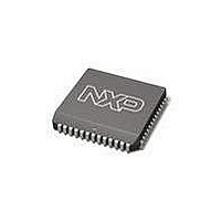
SC28C94A1A NXP Semiconductors, SC28C94A1A Datasheet - Page 22

SC28C94A1A
Manufacturer Part Number
SC28C94A1A
Description
UART Interface IC UART QUAD W/FIFO
Manufacturer
NXP Semiconductors
Type
Quad UARTr
Datasheet
1.SC28C94A1A512.pdf
(39 pages)
Specifications of SC28C94A1A
Number Of Channels
4
Data Rate
1 Mbps
Supply Voltage (max)
5.5 V
Supply Voltage (min)
4.5 V
Supply Current
35 mA
Maximum Operating Temperature
+ 85 C
Minimum Operating Temperature
- 40 C
Package / Case
PLCC-52
Description/function
Quad UART
Mounting Style
SMD/SMT
Operating Supply Voltage
5 V
Lead Free Status / Rohs Status
Details
Other names
SC28C94A1A,512
Available stocks
Company
Part Number
Manufacturer
Quantity
Price
Company:
Part Number:
SC28C94A1A,512
Manufacturer:
NXP Semiconductors
Quantity:
10 000
Company:
Part Number:
SC28C94A1A,518
Manufacturer:
Maxim
Quantity:
21
Company:
Part Number:
SC28C94A1A,518
Manufacturer:
NXP Semiconductors
Quantity:
10 000
Philips Semiconductors
I/O Port Control Channel B (IOPCRB)
I/O Port Control Channel C (IOPCRC)
I/O Port Control Channel D (IOPCRD)
The input part of the I/O pins is always active. The programming of the IOPCR bits to 00 merely turns off the out drivers and places
the pin at high impedance.
A read of the IPR register returns the value of the IPR bits as shown above. IPR(5) is at bit position 5 of the data bus. Note that the IPR bit
positions do not follow the 0, 1, 2, 3 order of the I/O ports. During a read of the IPR the I/O ports are not latched. Therefore, it is possible to see
changing data during the read. Port pins that have clocks on them may not yield valid data during the read.
Since the input circuits of the I/O ports are always active it is possible to direct the port signal back into the port. For example: I/O1 will output
the RTS signal. Setting the Counter/Timer (C/T) to be clocked by the I/O1 port will result in the counter counting the number of times RTS goes
active. The change of state detectors on I/O0 and I/O1 will, when programmed, always be sensitive to the signal on the port regardless of the
source of that port’s signal.
NOTES:
1. Normal configurations place RTSN output on I/O1 and place Tx external clock input on I/O3. For the 48 pin Dual In-Line package, I/O3 is
2. I/O1 becomes RTSN when IOPCR(3:2) = 01 and MR1(7) = 1 and OPR(1) = 1. (OPR(3) for channel B)
3. Recommended method for setting RTS/CTS flow control is to set IPCR [5:4] to 01 and to set I/OPCR[1:0] to 00. This makes I/O[2} RTSN
2006 Aug 09
00 = input
01 = output
10 = output
11 = output
00 = input
01 = output
10 = output
11 = output
00 = input
01 = output
10 = output
11 = output
Pin Control Bits
Pin Control Bits
Pin Control Bits
Quad universal asynchronous receiver/transmitter (QUART)
not available. The following options allow flexible I/O programming with the 48 pin package:
and I/O[1] CTSN. Caution: When RTS/CTS is active writing to the OPR register could conflict with the receiver control of OPR [6] and
OPR [4].
IOPCR[xx]
IOPCR[xx]
IOPCR[xx]
IPR(7), TxC in
OPRab(7)
TxC 16x
TxC 1x
IPR(5), TxC in
OPRcd(5)
TxC 16x
TxC 1x
IPR(7), TxC in
OPRcd(7)
TxC 16x
TxC 1x
When IOPCR(7:6), the I/O3 control,
When IOPCR(5:4), the I/O2 control, = 01, then I/O2 may be the RTSN signal if MR1(7) = 1 and OPR(4) = 1.
IOPCRb[7:6]
IOPCRc[7:6]
IOPCRd[7:6]
I/O3B
I/O3C
I/O3D
IPR(6), RxC in
OPRab(6)
RTSN
RxC 1x
RxC 16x
IPR(4), RxC in
OPRcd(4)
RTSN
RxC 1x
RxC 16x
IPR(6), RxC in
OPRcd(6)
RTSN
RxC 1x
RxC 16x
1
1
1
if IOPCR[5:4] = 01
if IOPCR[5:4] = 01
if IOPCR[5:4] = 01
IOPCRb[5:4]
IOPCRc[5:4]
IOPCRd[5:4]
00, then I/O1 becomes available to the transmitter as an external clock.
I/O2B
I/O2C
I/O2D
22
IPR(3), TxC in
OPRab(3)
RTSN
C/T ab out
RxC 1x
IPR(1), C/Tcd Clk in
OPRab(1)
RTSN
RxC 16x
RxC 1x
IPR(3), TxC in
OPRcd(3)
RTSN
C/T cd out
RxC 1x
2
2
2
if IOPCR[5:4]
if IOPCR[5:4]
if IOPCR[5:4]
IOPCRb[3:2]
IOPCRd[3:2]
IOPCRc[3:2]
I/O1B
I/O1C
I/O1D
1
TxC in
01
01
01
IPR(2), CTSN
OPRab(2)
TxC 1x
TxC 16x
IPR(0), CTSN
OPRcd(0)
TxC 1x
TxC 16x
IPR(2), CTSN
OPRcd(2)
TxC 1x
TxC 16x
IOPCRb[1:0]
IOPCRc[1:0]
IOPCRd[1:0]
SC28C94
Product data sheet
I/O0B
I/O0C
I/O0D


