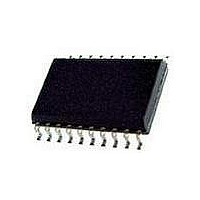
74HC9115D NXP Semiconductors, 74HC9115D Datasheet - Page 2

74HC9115D
Manufacturer Part Number
74HC9115D
Description
Buffers & Line Drivers NINE WIDE TRIG BUF
Manufacturer
NXP Semiconductors
Datasheet
1.74HCT9115D112.pdf
(7 pages)
Specifications of 74HC9115D
Logic Family
HC
Logic Type
CMOS
Number Of Channels Per Chip
9
Polarity
Non-Inverting
Supply Voltage (max)
6 V
Supply Voltage (min)
2 V
Maximum Operating Temperature
+ 125 C
Mounting Style
SMD/SMT
Package / Case
SOT-163-20
High Level Output Current
- 5.2 mA
Low Level Output Current
5.2 mA
Minimum Operating Temperature
- 40 C
Number Of Lines (input / Output)
9 / 9
Output Type
Open Drain
Propagation Delay Time
115 ns at 2 V
Lead Free Status / Rohs Status
Details
Other names
74HC9115D,112
Available stocks
Company
Part Number
Manufacturer
Quantity
Price
Company:
Part Number:
74HC9115D
Manufacturer:
PHILIPS
Quantity:
1 979
Philips Semiconductors
FEATURES
GENERAL DESCRIPTION
The 74HC/HCT9115 are high-speed Si-gate CMOS
devices and are pin compatible with low power Schottky
TTL (LSTTL). They are specified in compliance with
JEDEC standard no. 7A.
The 74HC/HCT9115 are nine wide Schmitt trigger buffer
with open drain outputs and Schmitt trigger inputs.
QUICK REFERENCE DATA
GND = 0 V; T
Notes
1. C
2. For HC the condition is V
ORDERING INFORMATION
See
December 1990
SYMBOL
t
C
C
PHL
Schmitt trigger action on all data inputs
Output capability: standard (open drain)
I
Nine wide Schmitt trigger buffer;
open drain outputs
I
PD
CC
f
f
C
V
For HCT the condition is V
i
o
“74HC/HCT/HCU/HCMOS Logic Package Information”
/ t
CC
PD
= input frequency in MHz
L
category: MSI
= output frequency in MHz
(C
PLZ
= output load capacitance in pF
P
= supply voltage in V
is used to determine the dynamic power dissipation (P
L
D
= C
V
amb
CC
PD
PARAMETER
propagation delay A
input capacitance
power dissipation capacitance per buffer
2
= 25 C; t
V
f
CC
o
) = sum of outputs
2
f
r
i
= t
I
I
f
= GND to V
= GND to V
= 6 ns
(C
L
n
to Y
V
CC
n
2
CC
CC
f
o
) where:
1.5 V
2
.
CONDITIONS
C
notes 1 and 2
The Schmitt trigger action in the data inputs transform
slowly changing input signals into sharply defined
jitter-free output signals.
The 74HC/HCT9115 have open-drain N-transistor
outputs, which are not clamped by a diode connected to
V
output may be pulled to any voltage between GND and
V
LOW-to-HIGH or HIGH-to-LOW level shifter. For digital
operation and OR-tied output applications, these devices
must have a pull-up resistor to establish a logic HIGH level.
The “9115” is identical to the “9114” but has non-inverting
outputs.
L
CC
Omax
D
= 15 pF; V
in W):
. In the OFF-state, i.e. when one input is HIGH, the
. This allows the device to be used as a
CC
= 5 V
12
3.5
5
74HC/HCT9115
HC
TYPICAL
Product specification
13
3.5
5
HCT
UNIT
ns
pF
pF


