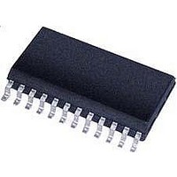
CS5523-AS Cirrus Logic Inc, CS5523-AS Datasheet - Page 13

CS5523-AS
Manufacturer Part Number
CS5523-AS
Description
ADC (A/D Converters) 4-Ch 16-Bit Delta Sigma ADC
Manufacturer
Cirrus Logic Inc
Datasheet
1.CS5521-ASZ.pdf
(56 pages)
Specifications of CS5523-AS
Architecture
Delta-Sigma
Conversion Rate
0.617 KSPs
Input Type
Voltage
Maximum Power Dissipation
500 mW
Maximum Operating Temperature
+ 85 C
Mounting Style
SMD/SMT
Package / Case
SOIC-8
Minimum Operating Temperature
- 40 C
Lead Free Status / Rohs Status
No
Available stocks
Company
Part Number
Manufacturer
Quantity
Price
Company:
Part Number:
CS5523-AS
Manufacturer:
HIT
Quantity:
1 200
Part Number:
CS5523-AS
Manufacturer:
CIRRUSLOGIC
Quantity:
20 000
Part Number:
CS5523-ASZ
Manufacturer:
CIRRUSLOGIC
Quantity:
20 000
1. GENERAL DESCRIPTION
The CS5521/22/23/24/28 are highly integrated ΔΣ
Analog-to-Digital Converters (ADCs) which use
charge-balance techniques to achieve 16-bit
(CS5521/23) and 24-bit (CS5522/24/28) perfor-
mance. The ADCs come as either two-channel
(CS5521/22), four-channel (CS5523/24), or eight-
channel (CS5528) devices, and include a low input
current, chopper-stabilized instrumentation ampli-
fier. To permit selectable input spans of 25 mV,
55 mV, 100 mV, 1 V, 2.5 V, and 5 V, the ADCs in-
clude a PGA (programmable gain amplifier). To
accommodate ground-based thermocouple applica-
tions, the devices include a CPD (Charge Pump
Drive) which provides a negative bias voltage to
the on-chip amplifiers.
These devices also include a fourth order DS mod-
ulator followed by a digital filter which provides
eight selectable output word rates of 1.88 Sps,
3.76 Sps, 7.51 Sps, 15 Sps, 30 Sps, 61.6 Sps,
84.5 Sps, and 101.1 Sps (XIN = 32.768 kHz). The
devices are capable of producing output update
rates up to 617 Sps when a 200 kHz clock is used
(CS5522/24/28) or up to 401 Sps using a 130 kHz
clock (CS5521/23). Further note that the digital fil-
DS317F8
AIN2+
AIN1+
AIN4+
AIN1+
AIN8+
AIN7+
AIN1+
AIN2-
AIN1-
AIN4-
AIN1-
NBV
*
*
*
*
*
*
CS5522
CS5524
CS5528
M
M
M
U
X
U
X
U
X
IN+
IN-
IN+
IN-
IN+
IN-
Figure 4. Multiplexer Configurations
IN+
IN-
X20
ters are designed to settle to full accuracy within
one conversion cycle and simultaneously reject
both 50 Hz and 60 Hz interference when operated
at word rates below 30 Sps (assuming a XIN clock
frequency of 32.768 kHz).
To ease communication between the ADCs and a
micro-controller, the converters include an easy to
use three-wire serial interface which is SPI™ and
Microwire™ compatible.
1.1 Analog Input
Figure 4 illustrates a block diagram of the analog in-
put signal path inside the CS5521/22/23/24/28. The
front end consists of a multiplexer (break before
make configuration), a chopper-stabilized instru-
mentation amplifier with fixed gain of 20X,
coarse/fine charge buffers, and a programmable gain
section. For the 25 mV, 55 mV, and 100 mV input
ranges, the input signals are amplified by the 20X in-
strumentation amplifier. For the 1 V, 2.5 V, and 5 V
input ranges, the instrumentation amplifier is by-
passed and the input signals are connected to the
Programmable Gain block via coarse/fine charge
buffers.
NBV also supplies the negative
supply voltage for the coarse/fine
change buffers
Programmable
Gain
VREF+
delta-sigma
Differential
modulator
4th order
VREF-
CS5521/22/23/24/28
Digital
Filter
13


