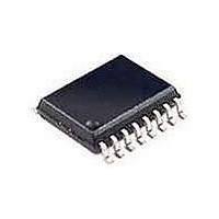
PCA9500D NXP Semiconductors, PCA9500D Datasheet - Page 16

PCA9500D
Manufacturer Part Number
PCA9500D
Description
I/O Expanders, Repeaters & Hubs I/O EXPANDER W/2K EE
Manufacturer
NXP Semiconductors
Datasheet
1.PCA9500PW112.pdf
(26 pages)
Specifications of PCA9500D
Logic Family
PCA
Number Of Lines (input / Output)
8 / 8
Operating Supply Voltage
2.5 V to 3.6 V
Operating Temperature Range
- 40 C to + 85 C
Package / Case
SOT-109
Mounting Style
SMD/SMT
Number Of Input Lines
8
Number Of Output Lines
8
Lead Free Status / Rohs Status
Details
Other names
PCA9500D,112
Available stocks
Company
Part Number
Manufacturer
Quantity
Price
Company:
Part Number:
PCA9500D
Manufacturer:
SHRP
Quantity:
3 116
Part Number:
PCA9500D
Manufacturer:
PHILIPS/飞利浦
Quantity:
20 000
NXP Semiconductors
12. Dynamic characteristics
Table 6.
[1]
[2]
[3]
Table 7.
PCA9500_4
Product data sheet
Symbol
I
f
t
t
t
t
t
t
t
t
t
t
Port timing
t
t
t
Power-up timing
t
t
Write cycle limits (see
T
Parameter
memory cell data retention
number of memory cell write cycles
2
SCL
SP
BUF
SU;STA
HD;STA
r
f
SU;DAT
HD;DAT
VD;DAT
SU;STO
v(Q)
su(D)
h(D)
pu(R)
pu(W)
cy(W)
C-bus timing
All the timing values are valid within the operating supply voltage and ambient temperature range and refer to V
voltage swing of V
t
guaranteed by design.
T
pu(R)
cy(W)
and t
is the maximum time that the device requires to perform the internal write operation.
Dynamic characteristics
Non-volatile storage specifications
pu(W)
Parameter
SCL clock frequency
pulse width of spikes that must be
suppressed by the input filter
bus free time between a STOP and START
condition
set-up time for a repeated START condition
hold time (repeated) START condition
rise time of both SDA and SCL signals
fall time of both SDA and SCL signals
data set-up time
data hold time
data valid time
set-up time for STOP condition
data output valid time
data input set-up time
data input hold time
read power-up time
write power-up time
write cycle time
[1]
(see
are the delays required from the time V
SS
to V
Figure
Figure
DD
.
22)
23)
Rev. 04 — 15 April 2009
DD
is stable until the specified operation can be initiated. These parameters are
Specification
10 years minimum
100,000 cycles minimum
Conditions
SCL LOW to
data output
C
C
C
8-bit I
L
L
L
100 pF
100 pF
100 pF
2
C-bus and SMBus I/O port with 2-kbit EEPROM
[2]
[2]
[3]
Min
-
-
1.3
0.6
0.6
-
-
250
0
-
0.6
-
0
4
-
-
-
Typ
-
-
-
-
-
-
-
-
-
-
-
-
-
-
-
-
5
PCA9500
IL
© NXP B.V. 2009. All rights reserved.
Max
400
50
-
-
-
0.3
0.3
-
-
1.0
-
4
-
-
1
5
10
and V
IH
with an input
Unit
kHz
ns
ns
ns
ms
ms
ms
16 of 26
s
s
s
s
s
s
s
s
s
s


