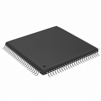
MAX9675ECQ+ Maxim Integrated Products, MAX9675ECQ+ Datasheet - Page 15

MAX9675ECQ+
Manufacturer Part Number
MAX9675ECQ+
Description
IC CROSSPOINT SWIT 16X16 100TQFP
Manufacturer
Maxim Integrated Products
Datasheet
1.MAX9675ECQT.pdf
(27 pages)
Specifications of MAX9675ECQ+
Function
Crosspoint Switch
Circuit
1 x 16:16
Voltage Supply Source
Single Supply
Voltage - Supply, Single/dual (±)
2.7 V ~ 5.5 V
Operating Temperature
-40°C ~ 85°C
Mounting Type
Surface Mount
Package / Case
100-TQFP Exposed Pad
Lead Free Status / RoHS Status
Lead free / RoHS Compliant
The MAX9675 is a highly integrated 16
ing video crosspoint switch matrix. All inputs and out-
puts are buffered, with all outputs able to drive
standard 75Ω reverse-terminated video loads.
A 3-wire interface programs the switch matrix and ini-
tializes with a single update signal. The unique serial
interface operates in one of two modes: Complete
Matrix Mode (Mode 1) or Individual Output Address
Mode (Mode 0).
In the Functional Diagram, the signal path of the
MAX9675 is from the inputs (IN0–IN15), through the
switching matrix, buffered by the output amplifiers, and
presented at the output terminals (OUT0–OUT15). The
other functional blocks are the serial interface and con-
trol logic. Each of the functional blocks is described in
detail below.
The MAX9675 outputs are high-speed voltage feedback
amplifiers capable of driving 150Ω (75Ω back-terminat-
ed) loads. The gain, A
through programming bit 4 of the serial control word.
______________________________________________________________________________________
RESET
UPDATE
V
Detailed Description
SCLK
IN15
DIN
IN0
IN1
IN2
= +1V/V or +2V/V, is selectable
CE
*A
V
= +1V/V OR +2V/V
POWER-ON
MAX9675
A0–A3 MODE
RESET
INTERFACE
SERIAL
110MHz, 16 x 16 Video Crosspoint
DISABLE ALL OUTPUTS
Analog Outputs
Switch with Programmable Gain
✕
SHUTDOWN
THERMAL
16 nonblock-
SWITCH MATRIX
MATRIX REGISTER
UPDATE REGISTER
DECODE LOGIC
LATCHES
16 x 16
96 BITS
16 BITS
256 16
Amplifier compensation is automatically optimized to
maximize the bandwidth for each gain selection. Each
output can be individually enabled and disabled through
bit 5 of the serial control word. When disabled, the out-
put is high impedance, presenting typically a 4kΩ load,
and 3pF output capacitance, allowing multiple outputs to
be connected together in building large arrays. On
power-up (or asynchronous RESET), all outputs are ini-
tialized in the disabled state to avoid output conflicts in
large-array configurations. The programming and opera-
tion of the MAX9675 is output referred. Outputs are con-
figured individually to connect to any one of the 16
analog inputs, programmed to the desired gain (A
+1V/V or +2V/V), or disabled in a high-impedance state.
The MAX9675 offers 16 analog input channels. Each
input is buffered before the crosspoint switch matrix,
allowing one input to cross-connect to up to 16 outputs.
The input buffers are voltage feedback amplifiers with
high-input impedance and low-input bias current. This
allows the use of very simple input clamp circuits.
16
A
A
A
A
V
V
V
V
*
*
*
*
Functional Diagram
OUT0
OUT1
OUT2
OUT15
V
V
AGND
DGND
DOUT
AOUT
V
CC
EE
DD
Analog Inputs
V
15
=


