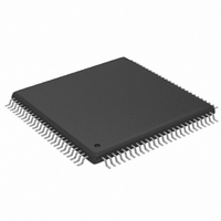
MAX9675ECQ+ Maxim Integrated Products, MAX9675ECQ+ Datasheet - Page 16

MAX9675ECQ+
Manufacturer Part Number
MAX9675ECQ+
Description
IC CROSSPOINT SWIT 16X16 100TQFP
Manufacturer
Maxim Integrated Products
Datasheet
1.MAX9675ECQT.pdf
(27 pages)
Specifications of MAX9675ECQ+
Function
Crosspoint Switch
Circuit
1 x 16:16
Voltage Supply Source
Single Supply
Voltage - Supply, Single/dual (±)
2.7 V ~ 5.5 V
Operating Temperature
-40°C ~ 85°C
Mounting Type
Surface Mount
Package / Case
100-TQFP Exposed Pad
Lead Free Status / RoHS Status
Lead free / RoHS Compliant
110MHz, 16 x 16 Video Crosspoint
Switch with Programmable Gain
The MAX9675 has 256 individual T-switches making a
16 x 16 switch matrix. The switching matrix is 100%
nonblocking, which means that any input may be rout-
ed to any output. The switch matrix programming is
output referred. Each output may be connected to any
one of the 16 analog inputs. Any one input can be rout-
ed to all 16 outputs with no signal degradation.
The digital interface consists of the following pins: DIN,
DOUT, SCLK, AOUT, UPDATE, CE, A3–A0, MODE, and
RESET. DIN is the serial-data input; DOUT is the serial-
data output. SCLK is the serial-data clock that clocks
data into the Data Input registers (Figure 2). Data at
DIN is loaded at each falling edge of SCLK. DOUT is
the data shifted out of the 96-bit Complete Matrix Mode
(Mode = 1). DIN passes directly to DOUT when in
Individual Output Address Mode (Mode = 0).
Table 1. Operation Truth Table
16
CE
1
0
0
0
0
X
______________________________________________________________________________________
UPDATE
X
X
1
0
1
0
SCLK
X
↓
X
↓
X
X
DIN
D
D
D
X
X
X
Digital Interface
i
i
i
Switch Matrix
DOUT
D
D
D
i-96
X
X
X
i
i
MODE
X
1
1
0
0
X
The falling edge of UPDATE latches the data and pro-
grams the matrix. When using Individual Output
Address Mode, the address recognition output AOUT
drives low when control word bits D13 to D10 match
the address programming inputs (A3–A0) and UPDATE
is low. Table 1 is the operation truth table.
The MAX9675 offers two programming modes:
Individual Output Address Mode and Complete Matrix
Mode. These two distinct programming modes are
selected by toggling a single MODE pin high or low.
Both modes operate with the same physical board lay-
out. This flexibility allows initial programming of the IC
by daisy-chaining and sending one long data word
while still being able to address immediately and
update individual outputs in the matrix.
Drive MODE to logic-low to select mode 0. Individual
outputs are programmed through the serial interface
AOUT
X
X
1
1
1
0
Individual Output Address Mode (MODE = 0)
RESET
1
1
1
1
1
0
No change in logic.
Data at DIN is clocked on the negative
edge of the SCLK into the 96-bit
Complete Matrix Mode register. DOUT
supplies original data in 96 SCLK
pulses later.
Data in the serial 96-bit Complete
Matrix Mode register is transferred
into parallel latches that control the
switching matrix.
Data at DIN is routed to the Individual
Output Address Mode shift register.
DIN is also connected directly to
DOUT so that all devices on the serial
bus may be addressed in parallel.
The 4-bit chip address A
compared to D
remaining 10 bits in the Individual
Output Address Mode register are
decoded, allowing reprogramming for
a single output. AOUT signals a
successful individual matrix update.
Asynchronous reset. All outputs are
disabled. Other logic remains
unchanged.
Programming the Matrix
OPERATION/COMMENTS
13
to D
10
. If equal, the
3
to A
0
is


