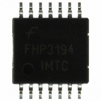
FHP3194IMTC14X Fairchild Semiconductor, FHP3194IMTC14X Datasheet - Page 12

FHP3194IMTC14X
Manufacturer Part Number
FHP3194IMTC14X
Description
MUX 4:1 ANALOG HI SPEED 14-TSSOP
Manufacturer
Fairchild Semiconductor
Datasheet
1.FHP3194IM14X.pdf
(17 pages)
Specifications of FHP3194IMTC14X
Function
Multiplexer
Circuit
1 x 4:1
Voltage Supply Source
Single Supply
Voltage - Supply, Single/dual (±)
5 V ~ 12 V
Operating Temperature
-40°C ~ 85°C
Mounting Type
Surface Mount
Package / Case
14-TSSOP
Lead Free Status / RoHS Status
Lead free / RoHS Compliant
Other names
FHP3194IMTC14XTR
© 2006 Fairchild Semiconductor Corporation
FHP3194 Rev. 1.0.1
Application Information
General Description
The FHP3194 4:1 multiplexer has four analog switches
that drive the positive input of a high-speed current
feedback amplifier. It is designed so that only one channel
is on at a time. Tie unused inputs to ground.
Figures 31 and 32 show typical application circuits for the
FHP3194 in 6dB (G = 2) and 0dB (G = 1) configurations.
R
The output of the FHP3194 is a current feedback amplifier.
The gain of this amplifier is set by two external resistors:
R
bandwidth of the current feedback amplifier are highly
dependant on the value of R
475Ω. For other gains, refer to the R
in Figure 3. In general, a lower R
response and increases bandwidth, while a higher R
decrease bandwidth and roll off the frequency response.
A feedback resistor is required for unity gain (G = 1); the
recommended value is 1.5kΩ.
A0, A1
The A0 and A1 logic pins are TTL/CMOS compatible and
are used to select which of the four inputs connects to
the output. Refer to the TRUTH TABLE on page 2 for
more information. Channel 1 is selected if both pins are
left floating.
EN, SD
The FHP3194 offers both shutdown and disable capability.
The EN (enable) pin is active low. During disable mode
(EN = 1), only the output amplifier is disabled, reducing
output glitches and allowing for multiplexer expansion.
The FHP3194 is enabled when the EN pin is left floating
or grounded.
The SD (shutdown) pin is active high. During shutdown
(SD = 1), the FHP3194 consumes only 2.5mA of supply
current. The FHP3194 is enabled when the SD pin is left
floating or grounded.
Supply Voltage
The FHP3194 operates from a single supply of 5V to
12V or dual supplies of ±2.5V to ±6.0V. For low supply
voltage operation, ensure that the common mode input
voltage range (CMIR) or output voltage range (V
exceeded. Exceeding the CMIR or V
FHP3194 into an overdrive condition. For example, the
typical CMIR for the FHP3194 is ±3.1V at ±5V supply,
which means 1.9V of headroom is required from each supply.
f
f
and R
and R
g
g
. The frequency response and closed-loop
Selection
f
. For a gain of two, use R
f
peaks the frequency
o
f
vs. GAIN plot
range puts the
o
) are not
f
will
f
=
1
At a single 5V supply, the CMIR becomes 1.9V to 3.1V. The
same theory can be applied to the V
Driving Video
The FHP3194 is designed to drive high-speed video.
90MHz 0.1dB bandwidth at 2V
differential gain/phase, and ±75mA output current make
the FHP3194 suitable for driving standard-definition, high-
definition, or PC graphics video.
Driving Video with a Single 5V Supply
The FHP3194 drives video signals from a single 5V supply
at G = 1 only. At higher gains, the CMIR and V
not suitable for passing video without clipping the signal.
Driving Capacitive Loads
The FREQUENCY RESPONSE VS. C
illustrates the response of the FHP3194. A small series
resistance (R
Figure 33, improves stability and settling performance. R
values in the FREQUENCY RESPONSE VS. C
chosen to achieve maximum bandwidth with less than 1dB
of peaking. For maximum flatness, use a larger R
Power Dissipation
The maximum internal power dissipation allowed is
directly related to the maximum junction temperature. If
the maximum junction temperature exceeds 150˚C for an
extended time, device failure may occur. The FHP3194 is
short-circuit protected; however, this may not guarantee
that the maximum junction temperature (+150˚C) is not
exceeded under all conditions. RMS power dissipation
can be calculated using the following equation:
Power Dissipation =
I
where I
pin voltage, V
is the RMS output voltage, and I
output current delivered to the load. Follow the maximum
power derating curves shown in Figure 34 to ensure proper
operation.
s
* (V
Figure 33. Typical Topology for Driving
s+
s
- V
is the supply current, V
s-
R
) + (V
g
s-
s
) at the output of the amplifier, illustrated in
is the negative supply pin voltage, V
-
+
Capacitive Loads
s+
- V
R
f
o(RMS)
R
) * I
s
s+
pp
OUT(RMS)
OUT(RMS)
OUT
is the positive supply
output, 0.02˚/0.05%
C
L
L
range.
plot in Figure 5,
R
www.fairchildsemi.com
L
is the RMS
L
o
plot were
s
range is
.
o(RMS)
s


