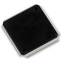
STM32F417IGT6 STMicroelectronics, STM32F417IGT6 Datasheet - Page 37

STM32F417IGT6
Manufacturer Part Number
STM32F417IGT6
Description
Microcontrollers (MCU) ARM M4 1024 FLASH 168 Mhz 192kB SRAM
Manufacturer
STMicroelectronics
Datasheet
1.STM32F417ZGT6.pdf
(168 pages)
Specifications of STM32F417IGT6
Core
ARM Cortex M4
Processor Series
STM32F4
Data Bus Width
32 bit
Maximum Clock Frequency
168 MHz
Program Memory Size
1024 KB
Data Ram Size
192 KB
On-chip Adc
Yes
Number Of Programmable I/os
140
Number Of Timers
10
Operating Supply Voltage
1.7 V to 3.6 V
Package / Case
LQFP-176
Mounting Style
SMD/SMT
A/d Bit Size
12 bit
A/d Channels Available
24
Interface Type
CAN, I2C, I2S, SPI, UART
Program Memory Type
Flash
Lead Free Status / Rohs Status
Details
Available stocks
Company
Part Number
Manufacturer
Quantity
Price
Company:
Part Number:
STM32F417IGT6
Manufacturer:
STMicroelectronics
Quantity:
413
- Current page: 37 of 168
- Download datasheet (3Mb)
STM32F415xx, STM32F417xx
2.2.36
2.2.37
2.2.38
2.2.39
The ADC can be served by the DMA controller. An analog watchdog feature allows very
precise monitoring of the converted voltage of one, some or all selected channels. An
interrupt is generated when the converted voltage is outside the programmed thresholds.
To synchronize A/D conversion and timers, the ADCs could be triggered by any of TIM1,
TIM2, TIM3, TIM4, TIM5, or TIM8 timer.
Temperature sensor
The temperature sensor has to generate a voltage that varies linearly with temperature. The
conversion range is between 1.8 V and 3.6 V. The temperature sensor is internally
connected to the ADC1_IN16 input channel which is used to convert the sensor output
voltage into a digital value.
As the offset of the temperature sensor varies from chip to chip due to process variation, the
internal temperature sensor is mainly suitable for applications that detect temperature
changes instead of absolute temperatures. If an accurate temperature reading is needed,
then an external temperature sensor part should be used.
Digital-to-analog converter (DAC)
The two 12-bit buffered DAC channels can be used to convert two digital signals into two
analog voltage signal outputs.
This dual digital Interface supports the following features:
●
●
●
●
●
●
●
●
●
●
Eight DAC trigger inputs are used in the device. The DAC channels are triggered through
the timer update outputs that are also connected to different DMA streams.
Serial wire JTAG debug port (SWJ-DP)
The ARM SWJ-DP interface is embedded, and is a combined JTAG and serial wire debug
port that enables either a serial wire debug or a JTAG probe to be connected to the target.
Debug is performed using 2 pins only instead of 5 required by the JTAG (JTAG pins could be
re-use as GPIO with alternate function): the JTAG TMS and TCK pins are shared with
SWDIO and SWCLK, respectively, and a specific sequence on the TMS pin is used to switch
between JTAG-DP and SW-DP.
Embedded Trace Macrocell™
The ARM Embedded Trace Macrocell provides a greater visibility of the instruction and data
flow inside the CPU core by streaming compressed data at a very high rate from the
two DAC converters: one for each output channel
8-bit or 12-bit monotonic output
left or right data alignment in 12-bit mode
synchronized update capability
noise-wave generation
triangular-wave generation
dual DAC channel independent or simultaneous conversions
DMA capability for each channel
external triggers for conversion
input voltage reference V
Doc ID 022063 Rev 2
REF+
Description
37/168
Related parts for STM32F417IGT6
Image
Part Number
Description
Manufacturer
Datasheet
Request
R

Part Number:
Description:
Microsoft .NET Micro Framework environment for STM32F4 microcontrollers
Manufacturer:
STMICROELECTRONICS [STMicroelectronics]
Datasheet:

Part Number:
Description:
DEV KIT FOR STM32
Manufacturer:
STMicroelectronics
Datasheet:

Part Number:
Description:
MCU ARM 128KB FLASH MEM 64-LQFP
Manufacturer:
STMicroelectronics
Datasheet:

Part Number:
Description:
MCU ARM 32BIT 128KB FLASH 64BGA
Manufacturer:
STMicroelectronics
Datasheet:

Part Number:
Description:
MCU ARM 32BIT 256K FLASH 144LQFP
Manufacturer:
STMicroelectronics
Datasheet:

Part Number:
Description:
KIT STARTER FOR STM32F10X
Manufacturer:
STMicroelectronics
Datasheet:

Part Number:
Description:
MCU ARM 128K FLASH/TIMER
Manufacturer:
STMicroelectronics
Datasheet:

Part Number:
Description:
MCU ARM 128KB FLASH MEM 100-LQFP
Manufacturer:
STMicroelectronics
Datasheet:

Part Number:
Description:
MCU 32BIT ARM 64K FLASH 36VFQFPN
Manufacturer:
STMicroelectronics
Datasheet:

Part Number:
Description:
MCU ARM 32BIT 32KB FLASH 48LQFP
Manufacturer:
STMicroelectronics
Datasheet:

Part Number:
Description:
MCU ARM 32BIT 64KB FLASH 64LQFP
Manufacturer:
STMicroelectronics
Datasheet:

Part Number:
Description:
MCU ARM 32BIT 384KB FLASH 64LQFP
Manufacturer:
STMicroelectronics
Datasheet:

Part Number:
Description:
MCU 32BIT ARM 512K FLASH 100-LQF
Manufacturer:
STMicroelectronics
Datasheet:

Part Number:
Description:
MCU ARM 32BIT 512KB FLASH 144BGA
Manufacturer:
STMicroelectronics
Datasheet:

Part Number:
Description:
MCU ARM 32BIT 512K FLASH 144LQFP
Manufacturer:
STMicroelectronics
Datasheet:


