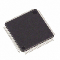
DS2152L+ Maxim Integrated Products, DS2152L+ Datasheet - Page 24

DS2152L+
Manufacturer Part Number
DS2152L+
Description
IC TXRX T1 1CHIP ENHNCD 100-LQFP
Manufacturer
Maxim Integrated Products
Datasheet
1.DS2152L.pdf
(97 pages)
Specifications of DS2152L+
Function
Single-Chip Transceiver
Interface
T1
Number Of Circuits
1
Voltage - Supply
4.75 V ~ 5.25 V
Current - Supply
75mA
Operating Temperature
0°C ~ 70°C
Mounting Type
Surface Mount
Package / Case
*
Includes
DSX-1 and CSU Line Build-Out Generator, HDLC Controller, In-Band Loop Code Generator and Detector
Lead Free Status / RoHS Status
Lead free / RoHS Compliant
Power (watts)
-
4.1 Payload Loopback
When CCR1.1 is set to 1, the DS2152 is forced into Payload Loopback (PLB). Normally, this loopback is
only enabled when ESF framing is being performed but can be enabled also in D4 framing applications.
In a PLB situation, the DS2152 loops the 192 bits of payload data (with BPVs corrected) from the receive
section back to the transmit section. The FPS framing pattern, CRC6 calculation, and the FDL bits are not
looped back, rather, they are reinserted by the DS2152. When PLB is enabled, the following occurs:
1) Data is transmitted from the TPOSO and TNEGO pins synchronous with RCLK instead of TCLK.
2) All the receive side signals continue to operate normally.
3) The TCHCLK and TCHBLK signals are forced low.
4) Data at the TSER, TDATA, and TSIG pins is ignored.
5) The TLCLK signal becomes synchronous with RCLK instead of TCLK.
4.2 Framer Loopback
When CCR1.0 is set to 1, the DS2152 enters a Framer Loopback (FLB) mode. This loopback is useful in
testing and debugging applications. In FLB, the DS2152 loops data from the transmit side back to the
receive side. When FLB is enabled, the following occurs:
1) An unframed all-1s code is transmitted at TPOSO and TNEGO.
2) Data at RPOSI and RNEGI is ignored.
3) All receive side signals take on timing synchronous with TCLK instead of RCLKI.
Note that it is not acceptable to have RCLK tied to TCLK during this loopback because this causes an
unstable condition.
4.3 Pulse Density Enforcer
The SCT always examines both the transmit and receive data streams for violations of the following rules
which are required by ANSI T1.403:
Violations for the transmit and receive data streams are reported in the RIR2.0 and RIR2.1 bits,
respectively. When the CCR3.3 is set to 1, the DS2152 forces the transmitted stream to meet this
requirement no matter the content of the transmitted stream. When running B8ZS, the CCR3.3 bit should
be set to 0 since B8ZS encoded data streams cannot violate the pulse density requirements.
4.4 Local Loopback
When CCR5.6 is set to 1, the DS2152 is forced into Local Loopback (LLB). In this loopback, data
continues to be transmitted as normal through the transmit side of the DS2152 (unless LIAIS = 1). Data
being received at RTIP and RRING is replaced with the data being transmitted. Data in this loopback
passes through the jitter attenuator. See
RCLKO tied to TCLKI during this loopback because this causes an unstable condition. Also, it is
recommended that the jitter attenuator be placed on the transmit side during this loopback.
•
•
No more than 15 consecutive 0s,
At least N 1s in each and every time window of 8 x (N + 1) bits where N = 1 through 23,
Figure 1-1
24 of 97
for more details. Note that it is not acceptable to have


