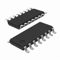
SI3200-BS Silicon Laboratories Inc, SI3200-BS Datasheet - Page 39

SI3200-BS
Manufacturer Part Number
SI3200-BS
Description
IC LINEFEED INTRFC 100V 16SOIC
Manufacturer
Silicon Laboratories Inc
Series
ProSLIC®r
Specifications of SI3200-BS
Function
Subscriber Line Interface Concept (SLIC), CODEC
Interface
GCI, PCM, SPI
Number Of Circuits
2
Voltage - Supply
3.3V, 5V
Current - Supply
110µA
Power (watts)
941mW
Operating Temperature
-40°C ~ 85°C
Mounting Type
Surface Mount
Package / Case
16-SOIC (3.9mm Width)
Includes
Battery Switching, BORSCHT Functions, DTMF Generation and Decoding, FSK Tone Generation, Modem and Fax Tone Detection
Lead Free Status / RoHS Status
Contains lead / RoHS non-compliant
Available stocks
Company
Part Number
Manufacturer
Quantity
Price
Company:
Part Number:
SI3200-BS
Manufacturer:
SILICON
Quantity:
1 082
Part Number:
SI3200-BS
Manufacturer:
N/A
Quantity:
20 000
Company:
Part Number:
SI3200-BSR
Manufacturer:
SILICON
Quantity:
14 000
In addition to the variable frequency and amplitude,
there is a selectable dc offset (V
to the waveform. The dc offset is defined in the RINGOF
RAM location. The ringing generator has two timers
which allow on/off cadence settings up to 8 s on/8 s off.
In addition to controlling ringing cadence, these timers
control the transition into and out of the ringing state.
To initiate ringing, the user must program the
RINGFREQ,
addresses as well as the RINGTA, and RINGTI
registers, and select the ringing waveshape and dc
offset. Once this is done, the TAEN and TIEN bits are
set as desired. Ringing state is invoked by a write to the
linefeed register. At the expiration of RINGTA, the
Si3232 turns off the ringing waveform and goes to the
on-hook transmission state. At the expiration of RINGTI,
ringing is initiated again. This process continues as long
as the two timers are enabled and the linefeed register
remains in the ringing state.
4.6.2. Internal Trapezoidal Ringing
In
waveform, the Si3232 can generate a trapezoidal
ringing waveform similar to the one illustrated in
Figure 19.
RINGPHAS RAM locations are used for programming
the ringing wave shape as follows:
RINGPHAS = 4 x Period x 8000
RINGAMP = (Desired V/160.8 V) x (2
RINGFREQ = (2 x RINGAMP) / (t
RINGFREQ is a value that is added or subtracted from
the waveform to ramp the signal up or down in a linear
fashion. This value is a function of rise time, period, and
amplitude, where rise time and period are related
through the following equation for the crest factor of a
trapezoidal waveform.
where
So, for a 90 V
crest factor of 1.3, the period is 0.05 s, and the rise time
requirement is 0.015 s.
RINGAMP
addition
=
The
1
-- -
4
T
CF
to
PK
RINGAMP,
=
-------------------- -
1.99211
, 20 Hz trapezoidal waveform with a
.00789
=
t
RISE
the
Period
desired crest factor
RINGFREQ,
=
traditional
×
3
-- - T 1
4
=
(
2
⎛
⎝
------------- -
f
15
and
RING
1
)
–
×
OFF
---------- -
CF
-------------------- -
160.173
RISE
1
2
RINGPHAS
85
) that can be added
sinusoidal
⎞
⎠
15
RINGAMP,
x 8000)
)
=
273
=
Preliminary Rev. 0.96
0x111
ringing
RAM
and
RINGPHAS = 4 x 0.05 x 8000 = 1600 (0x0640)
RINGAMP = 90/160.8 x (2
RINGFREQ = (2 x RINGAMP) (0.0153 x 8000) =
300 (0x012C)
The time registers and interrupts described in the
sinusoidal ring description also apply to the trapezoidal
ring waveform.
4.7. Internal Unbalanced Ringing
The Si3232 also provides the ability to generate a
traditional battery-backed unbalanced ringing waveform
for ringing terminating devices that require a high dc
content or for use in ground-start systems that cannot
tolerate a ringing waveform on both the TIP and RING
leads. The unbalanced ringing scheme applies the
ringing signal to the RING lead; the TIP lead remains at
the programmed VCM voltage that is very close to
ground. A programmable dc offset can be preset to
provide dc current for ring trip detection. Figure 18
illustrates the internal unbalanced ringing waveform.
To enable unbalanced ringing, set the RINGUNB bit of
the RINGCON register. As is the case with internal
balanced ringing, the unbalanced ringing waveform is
generated by using the on-chip ringing tone generator.
The tone generator used to generate ringing tones is a
two-pole resonator with programmable frequency and
amplitude. Since ringing frequencies are low compared
to the audio band signaling frequencies, the ringing
waveform is generated at a 1 kHz rate.
The ringing generator is programmed via the RINGAMP,
RINGFREQ, and RINGPHAS registers. The RINGOF
register is used to set the dc offset position around
V
-80V
GND
V
BATR
TIP
Si3232
Figure 18. Internal Unbalanced Ringing
V
OFF
V
DC Offset
RING
V
RING
15
) = 18340 (0x47A5)
DC Offset
V
V
CM
OVRING
RING
TIP
Si3232
39


