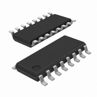
SI3200-BS Silicon Laboratories Inc, SI3200-BS Datasheet - Page 40

SI3200-BS
Manufacturer Part Number
SI3200-BS
Description
IC LINEFEED INTRFC 100V 16SOIC
Manufacturer
Silicon Laboratories Inc
Series
ProSLIC®r
Specifications of SI3200-BS
Function
Subscriber Line Interface Concept (SLIC), CODEC
Interface
GCI, PCM, SPI
Number Of Circuits
2
Voltage - Supply
3.3V, 5V
Current - Supply
110µA
Power (watts)
941mW
Operating Temperature
-40°C ~ 85°C
Mounting Type
Surface Mount
Package / Case
16-SOIC (3.9mm Width)
Includes
Battery Switching, BORSCHT Functions, DTMF Generation and Decoding, FSK Tone Generation, Modem and Fax Tone Detection
Lead Free Status / RoHS Status
Contains lead / RoHS non-compliant
Available stocks
Company
Part Number
Manufacturer
Quantity
Price
Company:
Part Number:
SI3200-BS
Manufacturer:
SILICON
Quantity:
1 082
Part Number:
SI3200-BS
Manufacturer:
N/A
Quantity:
20 000
Company:
Part Number:
SI3200-BSR
Manufacturer:
SILICON
Quantity:
14 000
Si3232
which the RING lead oscillates. The dc offset is set at a
dc point equal to V
the value that is input into the RINGOF RAM location.
Positive V
closer to ground (lower dc offset), and negative V
values have the opposite effect. The dc offset can be
set to any value; however, the ringing signal is clipped
digitally if the dc offset is set to a value that is less than
half the ringing amplitude. In general, the following
equation must hold true to ensure the battery voltage is
sufficient to provide the desired ringing amplitude:
|V
It is possible to create reverse polarity unbalanced
ringing waveforms (the TIP lead oscillates while the
RING lead stays constant) by setting the UNBPOLR bit
of the RINGCON register. In this mode, the polarity of
V
V
ringing V
4.7.1. Ringing Coefficients
The ringing coefficients are calculated in decimal for
sinusoidal and trapezoidal waveforms. The RINGPHAS
and
conversions in 16-bit, 2’s complement representations
for their respective RAM locations.
To obtain sinusoidal RINGFREQ RAM values, the
RINGFREQ decimal number is converted to a 24-bit 2’s
complement value. The lower 12 bits are placed in
RINGFRLO bits 14:3. RINGFRLO bits 15 and 2:0 are
cleared to 0. The upper 12 bits are set in a similar
manner in RINGFRHI, bits 13:3. RINGFRHI bit 14 is the
sign bit and RINGFRHI bits 2:0 are cleared to 0.
For
RINGFREQ = 0x7EFD9D are as follows:
RINGFRHI = 0x3F78
RINGFRLO = 0x6CE8
To obtain trapezoidal RINGFREQ RAM values, the
RINGFREQ decimal number is converted to an 8-bit, 2’s
complement value. This value is loaded into RINGFRHI.
RINGFRLO is not used.
40
OFF
OFF
BATR
must also be reversed (in normal ringing polarity,
is subtracted from –80 V, and in reverse polarity,
RINGAMP
| > |V
example,
OFF
OFF
RING,PK
is added to –80 V).
values cause the dc offset point to move
CM
hex
+ (–80 V + V
the
– (–80 V + V
values
register
OFF
are
OFF
) + V
), where V
OVRING
decimal-to-hex
values
Preliminary Rev. 0.96
|
OFF
OFF
for
is
4.7.2. Ringing DC Offset Voltage
A dc offset voltage can be added to the Si3232’s ac
ringing waveform by programming the RINGOF RAM
address to the appropriate setting. The value of
RINGOF is calculated as follows:
4.7.3. Linefeed Overhead Voltage Considerations
The ringing mode output impedance allows ringing
operation
(V
RING lead is desired, V
purpose.
4.7.4. Ringing Power Considerations
The total power consumption of the Si3232/Si3200
chipset using internal ringing generation is dependent
on the V
amplitude, the total loop impedance, and the ac load
impedance (number of REN). The following equations
can be used to approximate the total current required
for each channel during ringing mode.
Where:
OVR
Figure 19. Trapezoidal Ringing Waveform
During Ringing
= OV). If an offset of the ringing signal from the
V
TIP-RING
V
DD
R
without
Z
OFF
I
LOAD
LOOP
DD,AVE
V
supply voltage, the desired ringing
RING,PK
RINGOF
I
BAT,AVE
=
=
=
7000
------------ - (for North America)
REN
R
overhead
t
LOOP
V
---------------------- -
RISE
Z
=
RING,PK
=
LOOP
=
V
OVR
V
---------------------- -
RING,RMS
+
T=1/freq
-------------- -
160.8
Z
V
RING,PK
LOOP
R
OFF
×
LOAD
can be used for this
2
-- -
π
voltage
×
+
2
×
×
I
+
15
DD,OH
2
-- -
π
R
2
OUT
modification
time


