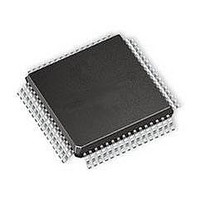
SI3232-KQ Silicon Laboratories Inc, SI3232-KQ Datasheet - Page 35

SI3232-KQ
Manufacturer Part Number
SI3232-KQ
Description
IC SLIC PROG DUAL-CH 64TQFP
Manufacturer
Silicon Laboratories Inc
Specifications of SI3232-KQ
Package / Case
*
Function
Subscriber Line Interface Concept (SLIC)
Interface
ISDN
Number Of Circuits
2
Voltage - Supply
3.13 V ~ 3.47 V
Current - Supply
28mA
Power (watts)
280mW
Operating Temperature
0°C ~ 70°C
Mounting Type
Surface Mount
Product
SLIC
Supply Voltage (min)
3.13 V
Supply Current
28 mA
Maximum Operating Temperature
+ 70 C
Minimum Operating Temperature
0 C
Mounting Style
SMD/SMT
Number Of Channels
2
Lead Free Status / RoHS Status
Contains lead / RoHS non-compliant
Available stocks
Company
Part Number
Manufacturer
Quantity
Price
Company:
Part Number:
SI3232-KQ
Manufacturer:
Silicon Laboratories Inc
Quantity:
10 000
Ringing Generation
The Si3232 is designed to provide a balanced ringing
waveform with or without dc offset. The ringing
frequency, cadence, waveshape, and dc offset are all
register-programmable.
Using a balanced ringing scheme, the ringing signal is
applied to both the TIP and the RING lines using ringing
waveforms that are 180° out of phase with each other.
The resulting ringing signal seen across TIP-RING is
twice the amplitude of the ringing waveform on either
the TIP or the RING line, which allows the ringing
circuitry to withstand only half the total ringing amplitude
seen across TIP-RING.
The purpose of an internal ringing scheme is to provide
>40 V
using a user-provided ringing battery supply. The
specific ringing supply voltage required depends on the
ringing voltage desired. The ringing amplitude at the
terminal equipment depends on the loop impedance as
well as the load impedance in REN. The following
equation can be used to determine the TIP-RING
ringing amplitude required for a specific load and loop
condition.
Figure 16. Balanced Ringing Waveform and
V
GND
BATH
rms
SLIC
V
V
into a 5 REN load at the terminal equipment
RING
TIP
V
PK
Components
V
V
RING
TIP
V
CM
V
OFF
V
OV
RING
TIP
Preliminary Rev. 0.95
V
OFF
where
When ringing longer loop lengths, adding a dc offset
voltage is necessary to reliably detect a ring trip
condition (off-hook phone). Adding dc offset to the
ringing signal decreases the maximum possible ringing
amplitude. Adding significant dc offset also increases
the power dissipation in the Si3200 and may require
additional airflow or a modified PCB layout to maintain
acceptable
automatically applies and removes the ringing signal
during V
crosstalk to adjacent lines. Table 21 provides a list of
registers required for internal ringing generation.
Figure 17. Simplified Loop Circuit During
R
OUT
V
R
V
TERM
LOOP
RING
OC
-crossing periods to reduce noise and
operating
=
=
V
0.09 Ω per foot for 26 AWG wire
RING
R
R
LOAD
OUT
×
Ringing
R
LOOP
----------------------------------------------------------------
R
temperatures.
=
=
LOAD
320 Ω
7000 Ω
------------------- -
#REN
+
R
R
LOAD
LOOP
R
LOAD
Si3232
+
R
The
OUT
V
Si3232
TERM
+
–
35


