DS2155G Maxim Integrated Products, DS2155G Datasheet - Page 62
DS2155G
Manufacturer Part Number
DS2155G
Description
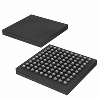
IC TXRX T1/E1/J1 1-CHIP 100CSBGA
Manufacturer
Maxim Integrated Products
Specifications of DS2155G
Function
Single-Chip Transceiver
Interface
E1, HDLC, J1, T1
Number Of Circuits
1
Voltage - Supply
3.14 V ~ 3.47 V
Current - Supply
75mA
Operating Temperature
0°C ~ 70°C
Mounting Type
Surface Mount
Package / Case
100-LFBGA
Includes
BERT Generator and Detector, CMI Coder and Decoder, HDLC Controller
Lead Free Status / RoHS Status
Contains lead / RoHS non-compliant
Power (watts)
-
Available stocks
Company
Part Number
Manufacturer
Quantity
Price

Part Number:
DS2155G+
Manufacturer:
MAXIM/ç¾ژن؟،
Quantity:
20 000
Company:
Part Number:
DS2155G+T&R
Manufacturer:
MAXIM
Quantity:
68
Company:
Part Number:
DS2155G+T&R
Manufacturer:
Maxim Integrated
Quantity:
10 000
Company:
Part Number:
DS2155G/T&R
Manufacturer:
Maxim Integrated
Quantity:
10 000
Part Number:
DS2155GN+
Manufacturer:
DALLAS
Quantity:
20 000
Company:
Part Number:
DS2155GNC2+T&R
Manufacturer:
MAXIM
Quantity:
14


11.
Register Name:
Register Description:
Register Address:
Bit #
Name
Default
Bit 0/Function of the RLOS/LOTC Output (RLOSF)
Bit 1/Transmit Clock Source Select Bit 0 (TCSS0)
Bit 2/Transmit Clock Source Select Bit 0 (TCSS1)
Bit 3/Disable Idle Code Auto Increment (DICAI). Selects/deselects the auto-increment feature for the transmit
and receive idle code array address register. See Section 17.
Bit 4/Output Data Mode (ODM)
Bit 5/Signaling Integration Enable (SIE)
Bit 6/CRC-4 Recalculate (CRC4R)
Bit 7/MCLK Source (MCLKS). Selects the source of MCLK
TCSS1
0
0
1
1
COMMON CONTROL AND STATUS REGISTERS
0 = receive loss of sync (RLOS)
1 = loss-of-transmit clock (LOTC)
0 = addresses in IAAR register automatically increment on every read/write operation to the PCICR
register
1 = addresses in IAAR register do not automatically increment
0 = pulses at TPOSO and TNEGO are one full TCLKO period wide
1 = pulses at TPOSO and TNEGO are one-half TCLKO period wide
0 = signaling changes of state reported on any change in selected channels
1 = signaling must be stable for three multiframes in order for a change of state to be reported
0 = transmit CRC-4 generation and insertion operates in normal mode
1 = transmit CRC-4 generation operates according to G.706 intermediate path recalculation method
0 = MCLK is source from the MCLK pin
1 = MCLK is source from the TSYSCLK pin
MCLKS
TCSS0
7
0
0
1
0
1
CRC4R
CCR1
Common Control Register 1
70h
The TCLK pin is always the source of transmit clock.
Switch to the clock present at RCLK when the signal at the TCLK pin
fails to transition after 1 channel time.
Use the scaled signal present at MCLK as the transmit clock. The
TCLK pin is ignored.
Use the signal present at RCLK as the transmit clock. The TCLK pin is
ignored.
6
0
SIE
5
0
ODM
4
0
Transmit Clock Source
62 of 238
DICAI
3
0
TCSS1
2
0
TCSS0
1
0
RLOSF
0
0
Related parts for DS2155G
Image
Part Number
Description
Manufacturer
Datasheet
Request
R

Part Number:
Description:
MAX7528KCWPMaxim Integrated Products [CMOS Dual 8-Bit Buffered Multiplying DACs]
Manufacturer:
Maxim Integrated Products
Datasheet:
Part Number:
Description:
Single +5V, fully integrated, 1.25Gbps laser diode driver.
Manufacturer:
Maxim Integrated Products
Datasheet:
Part Number:
Description:
Single +5V, fully integrated, 155Mbps laser diode driver.
Manufacturer:
Maxim Integrated Products
Datasheet:
Part Number:
Description:
VRD11/VRD10, K8 Rev F 2/3/4-Phase PWM Controllers with Integrated Dual MOSFET Drivers
Manufacturer:
Maxim Integrated Products
Datasheet:
Part Number:
Description:
Highly Integrated Level 2 SMBus Battery Chargers
Manufacturer:
Maxim Integrated Products
Datasheet:
Part Number:
Description:
Current Monitor and Accumulator with Integrated Sense Resistor; ; Temperature Range: -40°C to +85°C
Manufacturer:
Maxim Integrated Products
Part Number:
Description:
TSSOP 14/A°/RS-485 Transceivers with Integrated 100O/120O Termination Resis
Manufacturer:
Maxim Integrated Products
Part Number:
Description:
TSSOP 14/A°/RS-485 Transceivers with Integrated 100O/120O Termination Resis
Manufacturer:
Maxim Integrated Products
Part Number:
Description:
QFN 16/A°/AC-DC and DC-DC Peak-Current-Mode Converters with Integrated Step
Manufacturer:
Maxim Integrated Products
Part Number:
Description:
TDFN/A/65V, 1A, 600KHZ, SYNCHRONOUS STEP-DOWN REGULATOR WITH INTEGRATED SWI
Manufacturer:
Maxim Integrated Products
Part Number:
Description:
Integrated Temperature Controller f
Manufacturer:
Maxim Integrated Products
Part Number:
Description:
SOT23-6/I°/45MHz to 650MHz, Integrated IF VCOs with Differential Output
Manufacturer:
Maxim Integrated Products
Part Number:
Description:
SOT23-6/I°/45MHz to 650MHz, Integrated IF VCOs with Differential Output
Manufacturer:
Maxim Integrated Products
Part Number:
Description:
EVALUATION KIT/2.4GHZ TO 2.5GHZ 802.11G/B RF TRANSCEIVER WITH INTEGRATED PA
Manufacturer:
Maxim Integrated Products
Part Number:
Description:
QFN/E/DUAL PCIE/SATA HIGH SPEED SWITCH WITH INTEGRATED BIAS RESISTOR
Manufacturer:
Maxim Integrated Products
Datasheet: