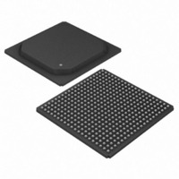
DS3172+ Maxim Integrated Products, DS3172+ Datasheet - Page 60

DS3172+
Manufacturer Part Number
DS3172+
Description
IC TXRX DS3/E3 DUAL 400-BGA
Manufacturer
Maxim Integrated Products
Datasheet
1.DS3171N.pdf
(234 pages)
Specifications of DS3172+
Function
Single-Chip Transceiver
Interface
DS3, E3
Number Of Circuits
2
Voltage - Supply
3.135 V ~ 3.465 V
Current - Supply
328mA
Operating Temperature
0°C ~ 70°C
Mounting Type
Surface Mount
Package / Case
400-BGA
Includes
DS3 Framers, E3 Framers, HDLC Controller, On-Chip BERTs
Lead Free Status / RoHS Status
Lead free / RoHS Compliant
Power (watts)
-
- Current page: 60 of 234
- Download datasheet (2Mb)
10.2.5 Gapped Clocks
The transmit and receive output clocks can be gapped in certain configurations. See
for the configuration settings. The gapped clocks are active during DS3 or E3 framed payload bits overhead bits
depending on which mode the device is configured for.
In the internal DS3 or E3 frame modes, the transmit gapped clock is created by the logical OR of the TCLKOn and
TDENn signals creating a positive or negative clock edge for each payload bit, the receive gapped clock is created
by the logical OR of the RCLKOn and RDENn signals.
When the output clock is disabled, the gapped output signal is high during clock periods if the pin is not inverted,
otherwise it will be low.
The gapped clocks are very useful when the data being clocked does not need to be aligned with any frame
structure. The data is simply clocked one bit at a time as a continuous data stream.
10.3 Reset and Power-Down
The device can be reset at a global level via the GL.CR1.RST bit or the RST pin and at the port level via the
PORT.CR1.RST bit and each port can be explicitly powered down via the PORT.CR1.PD bit. The JTAG logic is
reset using the power on reset signal from one of the LIUs as well as from the JTRST pin.
Figure 10-4. Example IO Pin Clock Muxing
TSER
TCLKI
RLCLK
CLAD CLOCKS
STS-1 CLK
RX LIU CLK
DS3 CLK
E3 CLK
PIN INVERT
PIN INVERT
PIN INVERT
DELAY
TFTS
0
1
CLOCK TREE
CLOCK TREE
CLOCK TREE
INTERNAL
INTERNAL
INTERNAL
SIGNAL
SIGNAL
SIGNAL
D
SET
CLR
Q
Q
60
D
D
D
D
SET
CLR
SET
CLR
SET
CLR
SET
CLR
Q
Q
Q
Q
Q
Q
Q
Q
INTERNAL
DELAY
SIGNAL
DELAY
DELAY
TFTS
TLTS
RFTS
0
1
0
1
0
1
D
D
D
SET
CLR
SET
CLR
SET
CLR
Q
Q
Q
Q
Q
Q
PIN INVERT
PIN INVERT
PIN INVERT
PIN INVERT
PIN INVERT
PIN INVERT
Table 10-22
RCLKO
TCLKO
TLCLK
TDEN
RSER
TPOS
and
Table 10-24
Related parts for DS3172+
Image
Part Number
Description
Manufacturer
Datasheet
Request
R

Part Number:
Description:
MAX7528KCWPMaxim Integrated Products [CMOS Dual 8-Bit Buffered Multiplying DACs]
Manufacturer:
Maxim Integrated Products
Datasheet:

Part Number:
Description:
Single +5V, fully integrated, 1.25Gbps laser diode driver.
Manufacturer:
Maxim Integrated Products
Datasheet:

Part Number:
Description:
Single +5V, fully integrated, 155Mbps laser diode driver.
Manufacturer:
Maxim Integrated Products
Datasheet:

Part Number:
Description:
VRD11/VRD10, K8 Rev F 2/3/4-Phase PWM Controllers with Integrated Dual MOSFET Drivers
Manufacturer:
Maxim Integrated Products
Datasheet:

Part Number:
Description:
Highly Integrated Level 2 SMBus Battery Chargers
Manufacturer:
Maxim Integrated Products
Datasheet:

Part Number:
Description:
Current Monitor and Accumulator with Integrated Sense Resistor; ; Temperature Range: -40°C to +85°C
Manufacturer:
Maxim Integrated Products

Part Number:
Description:
TSSOP 14/A�/RS-485 Transceivers with Integrated 100O/120O Termination Resis
Manufacturer:
Maxim Integrated Products

Part Number:
Description:
TSSOP 14/A�/RS-485 Transceivers with Integrated 100O/120O Termination Resis
Manufacturer:
Maxim Integrated Products

Part Number:
Description:
QFN 16/A�/AC-DC and DC-DC Peak-Current-Mode Converters with Integrated Step
Manufacturer:
Maxim Integrated Products

Part Number:
Description:
TDFN/A/65V, 1A, 600KHZ, SYNCHRONOUS STEP-DOWN REGULATOR WITH INTEGRATED SWI
Manufacturer:
Maxim Integrated Products

Part Number:
Description:
Integrated Temperature Controller f
Manufacturer:
Maxim Integrated Products

Part Number:
Description:
SOT23-6/I�/45MHz to 650MHz, Integrated IF VCOs with Differential Output
Manufacturer:
Maxim Integrated Products

Part Number:
Description:
SOT23-6/I�/45MHz to 650MHz, Integrated IF VCOs with Differential Output
Manufacturer:
Maxim Integrated Products

Part Number:
Description:
EVALUATION KIT/2.4GHZ TO 2.5GHZ 802.11G/B RF TRANSCEIVER WITH INTEGRATED PA
Manufacturer:
Maxim Integrated Products

Part Number:
Description:
QFN/E/DUAL PCIE/SATA HIGH SPEED SWITCH WITH INTEGRATED BIAS RESISTOR
Manufacturer:
Maxim Integrated Products
Datasheet:


