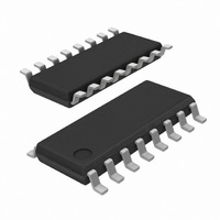
SI3200-FS Silicon Laboratories Inc, SI3200-FS Datasheet - Page 3

SI3200-FS
Manufacturer Part Number
SI3200-FS
Description
IC LINEFEED INTRFC 100V 16SOIC
Manufacturer
Silicon Laboratories Inc
Series
ProSLIC®r
Specifications of SI3200-FS
Package / Case
16-SOIC (3.9mm Width)
Function
Subscriber Line Interface Concept (SLIC), CODEC
Interface
GCI, PCM, SPI
Number Of Circuits
2
Voltage - Supply
3.3V, 5V
Current - Supply
110µA
Power (watts)
941mW
Operating Temperature
-40°C ~ 85°C
Mounting Type
Surface Mount
Includes
Battery Switching, BORSCHT Functions, DTMF Generation and Decoding, FSK Tone Generation, Modem and Fax Tone Detection
Product
SLIC
Supply Voltage (min)
3.13 V
Supply Current
0.11 mA, 8.8 mA
Maximum Operating Temperature
+ 70 C
Minimum Operating Temperature
0 C
Mounting Style
SMD/SMT
Number Of Channels
2
Lead Free Status / RoHS Status
Lead free / RoHS Compliant
Available stocks
Company
Part Number
Manufacturer
Quantity
Price
Part Number:
SI3200-FS
Manufacturer:
SILICON LABS/èٹ¯ç§‘
Quantity:
20 000
Company:
Part Number:
SI3200-FSR
Manufacturer:
SILICON
Quantity:
11 430
Maximum Si3200 Power Dissipation
The maximum power dissipation for the Si3200 linefeed
device is established from its specified maximum
junction temperature (T
thermal impedance (θ
supplied expected maximum ambient temperature
(T
Table 2 provides the thermal impedance of the Si3200
device and its maximum junction temperature.
To achieve the thermal impedance (θ
Table 2, it is necessary to provide a suitably-designed
PCB heat slug (copper fill) structure under the Si3200
package. The heat slug must be, as much as possible,
contiguous with the system GND fill on the top circuit
layer underneath the Si3200 package. The heat slug
should be connected with a row of eight vias that are at
least 10 mils (~0.25 mm) in diameter to inner PCB
circuit layers, such as the ground plane layer, and to the
bottom circuit side GND fill. The Si3220DC-EVB Rev. 2
evaluation board layout from Silicon Laboratories
provides an example of a suitable heat slug design for
the Si3200.
The primary objective of the power offload circuit is to
ensure that the power dissipation in the Si3200 device
will remain under P
ambient temperature under the required operating
conditions of loop length, battery voltage, loop current,
and bias current.
Optimal VBLO Determination
The power dissipation in the Si3200 device, during the
forward/reverse active off-hook state is obtained from
Equation 2 below.
where:
P
a(max)
Equation 2.Power Dissipated in Si3200 Linefeed
Si3200
Parameter
Equation 1.Maximum Power Dissipation
Table 2. Si3200 Thermal Parameters
).
T
j(max)
=
θ
ja
(
I
LIM
P
d max
(
+
I
BIAS
d(max)
)
=
) V
T
--------------------------------------------
ja
×
j(max)
j max
) along with the customer-
at up to the maximum required
(
BAT
Value
140
55
) and junction-to-ambient
)
θ
–
–
ja
T
(
R
a max
(
w
×
L
)
w
+
ja
R
°C/Watt
) stated in
ph
Units
°C
) I
×
LIM
2
Rev. 0.1
P
I
ILIM register in amps.
I
field in the SBIAS register in amps.
V
VBLO, depending on loop length) in volts.
R
the wire (e.g., 24AWG or 26AWG wire).
L
R
V
battery voltage the Si3200 is using. The Si322x devices
feature automatic battery selection, which is based
upon the measurement of the dc voltage present on the
RING terminal. "Battery Switching Threshold Settings‚"
on page 5 describes a method for selecting the correct
value for the BATHTH, BATLTH, and BATLPF RAM
locations, which control the voltage thresholds at which
the system will switch battery voltage and the filtering of
the RING dc signal. These RAM locations must be
programmed with the correct values that optimize the
switching point between VBHI and VBLO.
When the system is using the lower battery voltage
(VBLO), the worst-case power dissipation in the Si3200
occurs when the loop length is zero. If the loop length is
zero, the R
in Equation 3 .
Replacing P
with VBLO, an expression for VBLO is obtained as
shown in Equation 4.
Equation 4 yields the low battery voltage (VBLO) at
which the power dissipation in the Si3200 will equal
P
P
4 is modified to include a factor to scale P
provide margin, resulting in Equation 5. For example, let
k = 0.80 so that power dissipation in the Si3200 will be
at 80% of P
lim
bias
w
Si3200
BAT
ph
BAT
d(max)
Si3200
w
is the loop length in feet or meters.
is the resistance per linear foot (or linear meter) of
is the required off-hook loop current as set by the
is the off-hook dc resistance of the telephone.
is the required bias current as set by the ABIAS
Equation 3.Power Dissipated in the Si3200
may be either VBHI or VBLO depending on which
is the battery voltage (may be set to VBHI or
P
at zero loop length. Actually, it is desired to have
under P
is the power dissipated in the Si3200 in watts.
Si3200
w
d(max)
Si3200
x L
VBLO
=
d(max)
w
(at zero loop length)
(
I
when operating from VBLO on a zero
term in Equation 2 vanishes resulting
Equation 4.VBLO
LIM
in Equation 3 with P
=
by some margin. Hence, Equation
+
P
------------------------------------------------------- -
I
d max
BIAS
(
I
LIM
)
)
×
+
+
V
R
BAT
I
ph
BIAS
×
–
I
R
LIM
ph
d(max)
2
×
I
AN91
LIM
and V
d(max)
2
BAT
to
3


