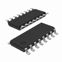
SI3200-FS Silicon Laboratories Inc, SI3200-FS Datasheet - Page 4

SI3200-FS
Manufacturer Part Number
SI3200-FS
Description
IC LINEFEED INTRFC 100V 16SOIC
Manufacturer
Silicon Laboratories Inc
Series
ProSLIC®r
Specifications of SI3200-FS
Package / Case
16-SOIC (3.9mm Width)
Function
Subscriber Line Interface Concept (SLIC), CODEC
Interface
GCI, PCM, SPI
Number Of Circuits
2
Voltage - Supply
3.3V, 5V
Current - Supply
110µA
Power (watts)
941mW
Operating Temperature
-40°C ~ 85°C
Mounting Type
Surface Mount
Includes
Battery Switching, BORSCHT Functions, DTMF Generation and Decoding, FSK Tone Generation, Modem and Fax Tone Detection
Product
SLIC
Supply Voltage (min)
3.13 V
Supply Current
0.11 mA, 8.8 mA
Maximum Operating Temperature
+ 70 C
Minimum Operating Temperature
0 C
Mounting Style
SMD/SMT
Number Of Channels
2
Lead Free Status / RoHS Status
Lead free / RoHS Compliant
Available stocks
Company
Part Number
Manufacturer
Quantity
Price
Part Number:
SI3200-FS
Manufacturer:
SILICON LABS/èٹ¯ç§‘
Quantity:
20 000
Company:
Part Number:
SI3200-FSR
Manufacturer:
SILICON
Quantity:
11 430
AN91
loop length line.
The selection of VBLO may require several iterations in
order to derive the optimal solution that ensures power
dissipation in both the Si3200 and the offload circuit
under all operating conditions. The “Power Offload Tool”
section of this document describes a Power Offload
Calculation tool to facilitate the iterative process to
determine the optimal VBLO.
Power Offload Circuit Component
Selection
Once the optimal VBLO has been determined, it is a
simple matter to determine the resistor value needed for
the resistive power offload circuit or the Zener diode
voltage for the linear regulator offload circuit.
Resistive Offload Circuit
The value of the resistor used in the resistive offload
circuit is readily computed from Equation 6.
Choose the standard 5% resistor value nearest to the
calculated R
The power dissipation in the offload resistor is obtained
from Equation 7:
Choose a resistor power rating that can accommodate
P
Linear Regulator Offload Circuit
The nominal Zener diode voltage is obtained from
VBLO, and the typical V
transistor.
Choose a 5% Zener diode with nominal Zener voltage
(Vz) as close as possible to the value determined by
Equation 8. Zener diodes in SOT23 packages are
4
offload
Equation 6.Offload Resistor Calculation
Equation 7.Resistor Power Dissipation
plus an adequate margin.
Equation 5.VBLO (with margin factor)
P
VBLO
offload
offload
V
Equation 8.Zener Voltage
R
z
offload
=
value.
=
=
VBHI
k P
-----------------------------------------------------------------
R
×
=
offload
------------------------------------------- -
d max
VBHI
be
–
(
I
LIM
I
LIM
VBLO
×
voltage drop in a bipolar
)
(
+
+
+
I
–
LIM
I
R
BIAS
I
VBLO
BIAS
ph
–
+
0.6V
×
I
BIAS
I
LIM
)
2
2
Rev. 0.1
typically rated at 350 mW, which is ample power
dissipation capacity for this application.
The power dissipated in the transistor used in the linear
regulator is obtained using Equation 9 (with both
channels simultaneously off-hook – hence the 2x factor
in Equation 9). The designer must ensure that the
selected transistor and its corresponding PCB footprint
can adequately handle the power dissipated with some
margin
manufacturer’s rated P
derating as ambient temperature increases. For most
applications, a PNP transistor, such as the ON
Semiconductor, MJD2955, in a DPAK package or
equivalent, is well suited for this application, provided
that a suitable PCB heat slug (copper fill) is designed
under the transistor package. (See "Typical Design
Example‚" on page 6).
Equation 10 provides the worst-case power dissipation
in the Zener diode based on the rated Zener voltage
and the rated minimum current gain (β
transistor for the case when both channels are
simultaneously off-hook. The Central Semiconductor
CMPZ4678-CMPZ4717 Zener diode family in an SOT-
23 package provides adequate power dissipating
margin. (See "Typical Design Example‚" on page 6).
Thermal Considerations
The system designer must carefully consider the PCB
placement of the offload resistor or the linear regulator
so as to optimize system heat dissipation. The offload
circuit (resistor or linear regulator) is not electrically
required to be placed close to pin 6 (VBATL) of the
Si3200 and should therefore be placed up to two inches
(approximately 5 cm) away from the Si3200 device,
thus, physically separating components that are
dissipating appreciable power.
To minimize the resistor cost, the offload resistors can
be through-hole instead of SMT. To further spread heat
dissipation and reduce the power rating of the individual
resistors, the offload resistors can be split into two or
more equal-value resistors whose parallel combination
forms the desired R
Equation 10.Zener Diode Power Dissipation
Equation 9.Transistor Power Dissipation
P
Q
while
=
2
×
P
(
Z
VBHI
taking
=
offload
2 V
×
–
d(max)
value.
Z
VBLO
×
into
I
----------------------------- -
LIM
and its corresponding
β
)
+
min
×
I
consideration
(
BIAS
I
LIM
+
I
BIAS
min
) of the
)
the


