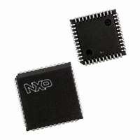
SC16C2550BIA44,512 NXP Semiconductors, SC16C2550BIA44,512 Datasheet - Page 19

SC16C2550BIA44,512
Manufacturer Part Number
SC16C2550BIA44,512
Description
IC UART DUAL W/FIFO 44-PLCC
Manufacturer
NXP Semiconductors
Datasheet
1.SC16C2550BIA44518.pdf
(43 pages)
Specifications of SC16C2550BIA44,512
Features
False-start Bit Detection
Number Of Channels
2, DUART
Fifo's
16 Byte
Voltage - Supply
3.5 V ~ 4.5 V
With Auto Flow Control
Yes
With False Start Bit Detection
Yes
With Modem Control
Yes
With Cmos
Yes
Mounting Type
Surface Mount
Package / Case
44-LCC (J-Lead)
Lead Free Status / RoHS Status
Lead free / RoHS Compliant
Other names
935274407512
SC16C2550BIA44
SC16C2550BIA44
SC16C2550BIA44
SC16C2550BIA44
Available stocks
Company
Part Number
Manufacturer
Quantity
Price
Company:
Part Number:
SC16C2550BIA44,512
Manufacturer:
NXP Semiconductors
Quantity:
10 000
NXP Semiconductors
SC16C2550B_5
Product data sheet
7.4 Interrupt Status Register (ISR)
Table 10.
Table 11.
The SC16C2550B provides four levels of prioritized interrupts to minimize external
software interaction. The Interrupt Status Register (ISR) provides the user with four
interrupt status bits. Performing a read cycle on the ISR will provide the user with the
highest pending interrupt level to be serviced. No other interrupts are acknowledged until
the pending interrupt is serviced. A lower level interrupt may be seen after servicing the
higher level interrupt and re-reading the interrupt status bits.
shows the data values (bits 3:0) for the four prioritized interrupt levels and the interrupt
sources associated with each of these interrupt levels.
Table 12.
Bit
1
0
FCR[7]
0
0
1
1
Priority
level
1
2
2
3
4
Symbol
FCR[1]
FCR[0]
ISR[3]
0
0
1
0
0
FIFO Control Register bits description
RCVR trigger levels
Interrupt source
FCR[6]
0
1
0
1
5 V, 3.3 V and 2.5 V dual UART, 5 Mbit/s (max.), with 16-byte FIFOs
ISR[2]
1
1
1
0
0
Description
RCVR FIFO reset.
FIFOs enabled.
Rev. 05 — 12 January 2009
logic 0 = Receive FIFO not reset (normal default condition)
logic 1 = clears the contents of the receive FIFO and resets the FIFO
counter logic (the Receive Shift Register is not cleared or altered). This
bit will return to a logic 0 after clearing the FIFO.
logic 0 = disable the transmit and receive FIFO (normal default
condition)
logic 1 = enable the transmit and receive FIFO. This bit must be a ‘1’
when other FCR bits are written to or they will not be programmed.
ISR[1]
1
0
0
1
0
RX FIFO trigger level
01
04
08
14
ISR[0]
0
0
0
0
0
Source of the interrupt
LSR (Receiver Line Status Register)
RXRDY (Received Data Ready)
RXRDY (Receive Data Time-out)
TXRDY (Transmitter Holding Register empty)
MSR (Modem Status Register)
…continued
Table 12 “Interrupt source”
SC16C2550B
© NXP B.V. 2009. All rights reserved.
19 of 43


