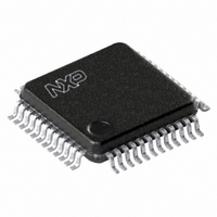
SC16C752BIB48,157 NXP Semiconductors, SC16C752BIB48,157 Datasheet - Page 8

SC16C752BIB48,157
Manufacturer Part Number
SC16C752BIB48,157
Description
IC UART DUAL W/FIFO 48-LQFP
Manufacturer
NXP Semiconductors
Type
Dual UART with 64-byte FIFOsr
Datasheet
1.SC16C752BIBS151.pdf
(47 pages)
Specifications of SC16C752BIB48,157
Number Of Channels
2, DUART
Package / Case
48-LQFP
Fifo's
64 Byte
Voltage - Supply
2.5V, 3.3V, 5V
With Auto Flow Control
Yes
With False Start Bit Detection
Yes
With Modem Control
Yes
Mounting Type
Surface Mount
Data Rate
5 Mbps
Supply Voltage (max)
5.5 V
Supply Voltage (min)
2.25 V
Supply Current
4.5 mA
Maximum Operating Temperature
+ 85 C
Minimum Operating Temperature
- 40 C
Mounting Style
SMD/SMT
Operating Supply Voltage
2.5 V or 3.3 V or 5 V
Lead Free Status / RoHS Status
Lead free / RoHS Compliant
Lead Free Status / RoHS Status
Lead free / RoHS Compliant, Lead free / RoHS Compliant
Other names
568-1322
935274411157
SC16C752BIB48
935274411157
SC16C752BIB48
Available stocks
Company
Part Number
Manufacturer
Quantity
Price
Company:
Part Number:
SC16C752BIB48,157
Manufacturer:
NXP Semiconductors
Quantity:
10 000
NXP Semiconductors
SC16C752B
Product data sheet
Fig 4.
Fig 5.
D7 to D0
Auto flow control (auto-RTS and auto-CTS) example
N = receiver FIFO trigger level.
The two blocks in dashed lines cover the case where an additional byte is sent, as described in
RTS functional timing
RTSn
RXn
IOR
6.2.1 Auto-RTS
Start
Auto-RTS data flow control originates in the receiver block (see
on page
in auto-RTS are stored in the TCR. RTSn is active if the RX FIFO level is below the halt
trigger level in TCR[3:0]. When the receiver FIFO halt trigger level is reached, RTSn is
de-asserted. The sending device (e.g., another UART) may send an additional byte after
the trigger level is reached (assuming the sending UART has another byte to send)
because it may not recognize the de-assertion of RTSn until it has begun sending the
additional byte. RTSn is automatically reasserted once the receiver FIFO reaches the
resume trigger level programmed via TCR[7:4]. This re-assertion allows the sending
device to resume transmission.
FIFO
FIFO
TX
RX
UART 1
byte N
3).
SERIAL TO
TO SERIAL
PARALLEL
PARALLEL
CONTROL
CONTROL
Figure 5
FLOW
FLOW
Stop
All information provided in this document is subject to legal disclaimers.
5 V, 2.2 V and 2.5 V dual UART, 5 Mbit/s (max.), with 64-byte FIFOs
shows RTSn functional timing. The receiver FIFO trigger levels used
Rev. 6 — 30 November 2010
RTSn
CTSn
Start
RXn
TXn
byte N + 1
1
TXn
CTSn
RXn
RTSn
2
Stop
SERIAL TO
TO SERIAL
PARALLEL
PARALLEL
CONTROL
CONTROL
FLOW
FLOW
UART 2
N
FIFO
FIFO
Section
Figure 1 “Block diagram”
SC16C752B
RX
TX
N+1
6.2.1.
002aaf905
© NXP B.V. 2010. All rights reserved.
Start
002aaf906
D7 to D0
8 of 47


