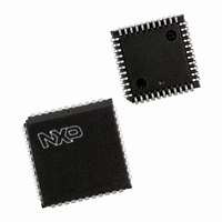
SCC2681AE1A44,529 NXP Semiconductors, SCC2681AE1A44,529 Datasheet - Page 11

SCC2681AE1A44,529
Manufacturer Part Number
SCC2681AE1A44,529
Description
IC UART DUAL 44-PLCC
Manufacturer
NXP Semiconductors
Type
Dual asynchronous receiver/transmitter (DUART)r
Datasheet
1.SCC2681AC1N40112.pdf
(29 pages)
Specifications of SCC2681AE1A44,529
Number Of Channels
2, DUART
Package / Case
44-LCC (J-Lead)
Features
False-start Bit Detection
Fifo's
3Bit
Voltage - Supply
4.5 V ~ 5.5 V
With Parallel Port
Yes
With Auto Flow Control
Yes
With False Start Bit Detection
Yes
With Cmos
Yes
Mounting Type
Surface Mount
Data Rate
0.1152 MBd
Supply Voltage (max)
5.5 V
Supply Voltage (min)
4.5 V
Supply Current
10 mA
Maximum Operating Temperature
+ 85 C
Minimum Operating Temperature
- 40 C
Mounting Style
SMD/SMT
Operating Supply Voltage
5 V
Lead Free Status / RoHS Status
Lead free / RoHS Compliant
Lead Free Status / RoHS Status
Lead free / RoHS Compliant, Lead free / RoHS Compliant
Other names
568-3526-5
935274518529
SCC2681AE1A44-S
935274518529
SCC2681AE1A44-S
Available stocks
Company
Part Number
Manufacturer
Quantity
Price
Company:
Part Number:
SCC2681AE1A44,529
Manufacturer:
NXP Semiconductors
Quantity:
10 000
The operation of the DUART is programmed by writing control words
Philips Semiconductors
PROGRAMMING
into the appropriate registers. Operational feedback is provided via
status registers which can be read by the CPU. The addressing of
the registers is described in Table 1.
The contents of certain control registers are initialized to zero on
RESET. Care should be exercised if the contents of a register are
changed during operation, since certain changes may cause
operational problems.
For example, changing the number of bits per character while the
transmitter is active may cause the transmission of an incorrect
character. In general, the contents of the MR, the CSR, and the
OPCR should only be changed while the receiver(s) and
transmitter(s) are not enabled, and certain changes to the ACR
should only be made while the C/T is stopped.
Table 1. SCC2681 Register Addressing
* See Table 5 for BRG Extended frequencies in this data sheet, and “Extended baud rates for SCN2681, SCN68681, SCC2691, SCC2692,
SCC68692 and SCC2698B” in application notes elsewhere in this publication.
2004 Apr 06
Dual asynchronous receiver/transmitter (DUART)
A3
0
0
0
0
0
0
0
0
1
1
1
1
1
1
1
1
A2
0
0
0
0
1
1
1
1
0
0
0
0
1
1
1
1
A1
0
0
1
1
0
0
1
1
0
0
1
1
0
0
1
1
A0
0
1
0
1
0
1
0
1
0
1
0
1
0
1
0
1
Mode Register A (MR1A, MR2A)
Status Register A (SRA)
BRG Extend *
Rx Holding Register A (RHRA)
Input Port Change Register (IPCR)
Interrupt Status Register (ISR)
Counter/Timer Upper Value (CTU)
Counter/Timer Lower Value (CTL)
Mode Register B (MR1B, MR2B)
Status Register B (SRB)
1 /16 Test
Rx Holding Register B (RHRB)
Use for scratch pad
Input Ports IP0 to IP6
Start Counter Command
Stop Counter Command
READ (RDN = 0)
11
The pointer then remains at MR2x, so that subsequent accesses are
Mode registers 1 and 2 of each channel are accessed via
independent auxiliary pointers. The pointer is set to MR1x by
RESET or by issuing a ‘reset pointer’ command via the
corresponding command register. Any read or write of the mode
register while the pointer is at MR1x, switches the pointer to MR2x.
always to MR2x unless the pointer is reset to MR1x as described
above.
Mode, command, clock select, and status registers are duplicated
for each channel to provide total independent operation and control.
Refer to Table 2 for register bit descriptions.
Mode Register A (MR1A, MR2A)
Clock Select Register A (CSRA)
Command Register A (CRA)
Tx Holding Register A (THRA)
Aux. Control Register (ACR)
Interrupt Mask Register (IMR)
C/T Upper Preset Value (CRUR)
C/T Lower Preset Value (CTLR)
Mode Register B (MR1B, MR2B)
Clock Select Register B (CSRB)
Command Register B (CRB)
Tx Holding Register B (THRB)
Use for scratch pad
Output Port Conf. Register (OPCR)
Set Output Port Bits Command
Reset Output Port Bits Command
WRITE (WRN = 0)
SCC2681
Product data


