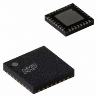
SC16C550BIBS,128 NXP Semiconductors, SC16C550BIBS,128 Datasheet - Page 7

SC16C550BIBS,128
Manufacturer Part Number
SC16C550BIBS,128
Description
IC UART SOT617-1
Manufacturer
NXP Semiconductors
Datasheet
1.SC16C550BIA44518.pdf
(48 pages)
Specifications of SC16C550BIBS,128
Features
Programmable
Number Of Channels
1, UART
Fifo's
16 Byte
Voltage - Supply
2.5V, 3.3V, 5V
With Auto Flow Control
Yes
With False Start Bit Detection
Yes
With Modem Control
Yes
With Cmos
Yes
Mounting Type
Surface Mount
Package / Case
32-VFQFN Exposed Pad
Lead Free Status / RoHS Status
Lead free / RoHS Compliant
Other names
935279497128
SC16C550BIBS-F
SC16C550BIBS-F
SC16C550BIBS-F
SC16C550BIBS-F
NXP Semiconductors
Table 2.
SC16C550B_5
Product data sheet
Symbol
DSR
DTR
INT
n.c.
OUT1
OUT2
RCLK
IOR
IOR
RESET
[2]
[2]
Pin description
Pin
PLCC44 LQFP48 DIP40 HVQFN32
41
37
33
1, 12,
23, 34
38
35
10
25
24
39
39
33
30
1, 6, 13,
21, 25,
36, 37,
48
34
31
5
20
19
35
…continued
37
33
30
-
34
31
9
22
21
35
25
22
20
2, 15, 16
-
-
-
-
14
23
Rev. 05 — 1 October 2008
Type
I
O
O
-
O
I
I
I
Description
Data set ready. DSR is a modem status signal. Its
condition can be checked by reading bit 5 (DSR) of the
Modem Status Register. Bit 1 (DSR) of the Modem Status
Register indicates DSR has changed levels since the last
read from the Modem Status Register. If the modem status
interrupt is enabled when DSR changes levels, an interrupt
is generated.
Data terminal ready. When active (LOW), DTR informs a
modem or data set that the UART is ready to establish
communication. DTR is placed in the active level by setting
the DTR bit of the Modem Control Register. DTR is placed
in the inactive level either as a result of a Master Reset,
during loopback mode operation, or clearing the DTR bit.
Interrupt. When active (HIGH), INT informs the CPU that
the UART has an interrupt to be serviced. Four conditions
that cause an interrupt to be issued are: a receiver error,
received data that is available or timed out (FIFO mode
only), an empty Transmitter Holding Register or an
enabled modem status interrupt. INT is reset (deactivated)
either when the interrupt is serviced or as a result of a
Master Reset.
not connected
Outputs 1 and 2. These are user-designated output
terminals that are set to the active (LOW) level by setting
respective Modem Control Register (MCR) bits (OUT1 and
OUT2). OUT1 and OUT2 are set to inactive the (HIGH)
level as a result of Master Reset, during loopback mode
operations, or by clearing bit 2 (OUT1) or bit 3 (OUT2) of
the MCR.
Receiver clock. RCLK is the 16 baud rate clock for the
receiver section of the UART. In the HVQFN32 package,
BAUDOUT and RCLK are bonded internally.
Read inputs. When either IOR or IOR is active (LOW or
HIGH, respectively) while the UART is selected, the CPU
is allowed to read status information or data from a
selected UART register. Only one of these inputs is
required for the transfer of data during a read operation;
the other input should be tied to its inactive level (that is,
IOR tied LOW or IOR tied HIGH).
Master reset. When active (HIGH), RESET clears most
UART registers and sets the levels of various output
signals.
5 V, 3.3 V and 2.5 V UART with 16-byte FIFOs
SC16C550B
© NXP B.V. 2008. All rights reserved.
7 of 48


