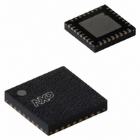
SC16C852LIBS,157 NXP Semiconductors, SC16C852LIBS,157 Datasheet - Page 9

SC16C852LIBS,157
Manufacturer Part Number
SC16C852LIBS,157
Description
IC UART DUAL W/FIFO 32-HVQFN
Manufacturer
NXP Semiconductors
Datasheet
1.SC16C852LIBS151.pdf
(64 pages)
Specifications of SC16C852LIBS,157
Features
Programmable
Number Of Channels
2, DUART
Fifo's
128 Byte
Protocol
RS485
Voltage - Supply
1.8V
With Auto Flow Control
Yes
With Irda Encoder/decoder
Yes
With False Start Bit Detection
Yes
With Modem Control
Yes
With Cmos
Yes
Mounting Type
Surface Mount
Package / Case
32-VFQFN Exposed Pad
Lead Free Status / RoHS Status
Lead free / RoHS Compliant
Other names
935283101157
SC16C852LIBS
SC16C852LIBS
SC16C852LIBS
SC16C852LIBS
NXP Semiconductors
Table 2.
SC16C852L
Product data sheet
Symbol
INTA/IRQ
INTB/n.c.
IOR/V
IOW/R/W
OP2A
OP2B
RESET/
RESET
RIA
RIB
RTSA
RTSB
DD
Pin description
Pin
LQFP48
30
29
19
15
32
9
36
41
21
33
22
HVQFN32 TFBGA36
22
21
14
12
-
-
24
-
-
23
15
…continued
C5
C6
F4
F3
-
-
A6
-
-
B6
F5
All information provided in this document is subject to legal disclaimers.
1.8 V dual UART with 128-byte FIFOs and IrDA encoder/decoder
Type
O
O
I
I
O
O
I
I
I
O
O
Rev. 4 — 1 February 2011
Description
When 16/68 pin is at logic 1 or unconnected, this output becomes
channel A interrupt output. The output state is defined by the user
through the software setting of MCR[3]. INTA is set to the active
mode and OP2A output to a logic 0 when MCR[3] is set to a
logic 1. INTA is set to the 3-state mode and OP2A is set to a logic 1
when MCR[3] is set to a logic 0.
When 16/68 pin is at logic 0, this output becomes device interrupt
output (active LOW, open-drain). An external pull-up resistor to
V
When 16/68 pin is at logic 1 or unconnected, this output becomes
channel B interrupt output. The output state is defined by the user
through the software setting of MCR[3]. INTB is set to the active
mode and OP2B output to a logic 0 when MCR[3] is set to a
logic 1. INTB is set to the 3-state mode and OP2B is set to a
logic 1 when MCR[3] is set to a logic 0.
When 16/68 pin is at logic 0, this output is not used.
When 16/68 pin is at logic 1, this input becomes the read strobe
(active LOW). When 16/68 pin is at logic 0, this input pin is not
used and should be connected to V
When 16/68 pin is at logic 1 or unconnected, this input becomes
the write strobe (active LOW).
When 16/68 pin is at logic 0, this input becomes read strobe when
it is at logic HIGH, and write strobe when it is at logic LOW.
Output 2 (user-defined). This function is associated with
individual channels, A through B. The state at these pin(s) are
defined by the user and through MCR register bit 3. INTA, INTB
are set to the active mode and OP2x to logic 0 when MCR[3] is set
to a logic 1. INTA, INTB are set to the 3-state mode and OP2x to a
logic 1 when MCR[3] is set to a logic 0 (see
Control Register bits
both the INTA, INTB operation and OP2x outputs, only one
function should be used at one time, INT or OP2.
Master Reset. When 16/68 pin is at logic 1 or unconnected, this
input becomes the RESET pin (active HIGH).
When 16/68 pin is at logic LOW, this input pin becomes RESET
(active LOW). (See
condition and software reset”
Ring Indicator (active LOW). These inputs are associated with
individual UART channels, A through B. A logic 0 on this pin
indicates the modem has received a ringing signal from the
telephone line. A logic 1 transition on this input pin will generate an
interrupt if modem status interrupt is enabled.
Request to Send (active LOW). These outputs are associated
with individual UART channels, A through B. A logic 0 on the RTSx
pin indicates the transmitter has data ready and waiting to send.
Writing a logic 1 in the modem control register MCR[1] will set this
pin to a logic 0, indicating data is available. After a reset this pin
will be set to a logic 1.
DD
is required.
Section 7.23 “SC16C852L external reset
description”, bit 3). Since these bits control
for initialization details.)
DD
.
SC16C852L
Table 21 “Modem
© NXP B.V. 2011. All rights reserved.
9 of 64


