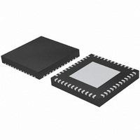
SC16C852VIBS,557 NXP Semiconductors, SC16C852VIBS,557 Datasheet - Page 14

SC16C852VIBS,557
Manufacturer Part Number
SC16C852VIBS,557
Description
IC UART DUAL W/FIFO 48-HVQFN
Manufacturer
NXP Semiconductors
Datasheet
1.SC16C852VIBS557.pdf
(55 pages)
Specifications of SC16C852VIBS,557
Features
Programmable
Number Of Channels
2, DUART
Fifo's
128 Byte
Protocol
RS485
Voltage - Supply
1.8V
With Auto Flow Control
Yes
With Irda Encoder/decoder
Yes
With False Start Bit Detection
Yes
With Modem Control
Yes
With Cmos
Yes
Mounting Type
Surface Mount
Package / Case
48-VQFN Exposed Pad, 48-HVQFN, 48-SQFN, 48-DHVQFN
Lead Free Status / RoHS Status
Lead free / RoHS Compliant
Other names
935283102557
SC16C852VIBS
SC16C852VIBS
SC16C852VIBS
SC16C852VIBS
NXP Semiconductors
SC16C852V
Product data sheet
6.9 Programmable baud rate generator
The SC16C852V UART contains a programmable rational baud rate generator that takes
any clock input and divides it by a divisor in the range between 1 and (2
SC16C852V offers the capability of dividing the input frequency by rational divisor. The
fractional part of the divisor is controlled by the CLKPRES register in the First Extra
Register Set.
where:
Prescaler = 1 when MCR[7] is set to 0.
Prescaler = 4 when MCR[7] is set to 1.
A single baud rate generator is provided for the transmitter and receiver. The
programmable Baud Rate Generator (BRG) is capable of operating with a frequency of up
to 80 MHz. To obtain maximum data rate, it is necessary to use full rail swing on the clock
input. The SC16C852V can be configured for internal or external clock operation. For
internal clock operation, an industry standard crystal is connected externally between the
XTAL1 and XTAL2 pins (see
to the XTAL1 pin (see
custom rates (see
The generator divides the input 16× clock by any divisor from 1 to (2
SC16C852V divides the basic external clock by 16. The baud rate is configured via the
CLKPRES, DLL and DLM internal register functions. Customized baud rates can be
achieved by selecting the proper divisor values for the MSB and LSB sections of the baud
rate generator.
Programming the baud rate generator registers CLKPRES, DLM (MSB) and DLL (LSB)
provides a user capability for selecting the desired final baud rate. The example in
shows the selectable baud rate available when using a 1.8432 MHz external clock input
with MCR[7] is 0, and CLKPRES = 0x00.
baud rate
Fig 6.
N is the integer part of the divisor in DLL and DLM registers;
M is the fractional part of the divisor in CLKPRES register;
f
XTAL1
XTAL1
XTAL2
is the clock frequency at XTAL1 pin.
Prescalers and baud rate generator block diagram
=
OSCILLATOR
------------------------------------------------------------------ -
MCR 7 [ ]
Dual UART with 128-byte FIFOs, IrDA, and XScale VLIO bus interface
All information provided in this document is subject to legal disclaimers.
Table
×
Figure
Rev. 5 — 21 January 2011
f
XTAL1
6).
16
×
DIVIDE-BY-1
DIVIDE-BY-4
Figure
8) to clock the internal baud rate generator for standard or
⎛
⎝
N
+
----- -
16
M
7). Alternatively, an external clock can be connected
⎞
⎠
MCR[7] = 0
MCR[7] = 1
GENERATOR
BAUD RATE
(DLL, DLM)
CLKPRES
[3:0]
SC16C852V
16
− 1). The
© NXP B.V. 2011. All rights reserved.
16
− 1). The
transmitter and
receiver clock
002aac645
Table 6
14 of 55
(1)


