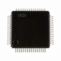
SC16C750BIB64,128 NXP Semiconductors, SC16C750BIB64,128 Datasheet - Page 10

SC16C750BIB64,128
Manufacturer Part Number
SC16C750BIB64,128
Description
IC UART 64BYTE 64LQFP
Manufacturer
NXP Semiconductors
Datasheet
1.SC16C750BIA44518.pdf
(44 pages)
Specifications of SC16C750BIB64,128
Number Of Channels
1, UART
Fifo's
64 Byte
Voltage - Supply
2.5V, 3.3V, 5V
With Auto Flow Control
Yes
With False Start Bit Detection
Yes
With Modem Control
Yes
With Cmos
Yes
Mounting Type
Surface Mount
Package / Case
64-LQFP
Lead Free Status / RoHS Status
Lead free / RoHS Compliant
Other names
935274403128
SC16C750BIB64-F
SC16C750BIB64-F
SC16C750BIB64-F
SC16C750BIB64-F
Available stocks
Company
Part Number
Manufacturer
Quantity
Price
Company:
Part Number:
SC16C750BIB64,128
Manufacturer:
NXP Semiconductors
Quantity:
10 000
NXP Semiconductors
SC16C750B_5
Product data sheet
6.2 FIFO operation
6.3 Hardware flow control
6.4 Time-out interrupts
The 64-byte transmit and receive data FIFOs are enabled by the FIFO Control Register
bit 0 (FCR[0]). The receiver FIFO section includes a time-out function to ensure data is
delivered to the external CPU. An interrupt is generated whenever the Receive Holding
Register (RHR) has not been read following the loading of a character or the receive
trigger level has not been reached.
Table 4.
When automatic hardware flow control is enabled, the SC16C750B monitors the CTS pin
for a remote buffer overflow indication and controls the RTS pin for local buffer overflows.
Automatic hardware flow control is selected by setting MCR[5] (RTS) and MCR[1] (CTS)
to a logic 1. If CTS transitions from a logic 0 to a logic 1 indicating a flow control request,
the SC16C750B will suspend TX transmissions as soon as the stop bit of the character in
process is shifted out. Transmission is resumed after the CTS input returns to a logic 0,
indicating more data may be sent.
With the auto-RTS function enabled, an interrupt is generated when the receive FIFO
reaches the programmed trigger level. The RTS pin will not be forced to a logic 1 (RTS
off), until the receive FIFO reaches the next trigger level. However, the RTS pin will return
to a logic 0 after the data buffer (FIFO) is emptied. However, under the above described
conditions, the SC16C750B will continue to accept data until the receive FIFO is full.
When two interrupt conditions have the same priority, it is important to service these
interrupts correctly. Receive Data Ready and Receive Time-Out have the same interrupt
priority (when enabled by IER[0]). The receiver issues an interrupt after the number of
characters have reached the programmed trigger level. In this case, the SC16C750B
FIFO may hold more characters than the programmed trigger level. Following the removal
of a data byte, the user should re-check LSR[0] for additional characters. A Receive
Time-Out will not occur if the receive FIFO is empty. The time-out counter is reset at the
center of each stop bit received or each time the receive holding register (RHR) is read.
The actual time-out value is 4 character time.
Selected trigger level
(characters)
16-byte FIFO
1
4
8
14
64-byte FIFO
1
16
32
56
Flow control mechanism
Rev. 05 — 17 October 2008
INT pin activation
1
4
8
14
1
16
32
56
5 V, 3.3 V and 2.5 V UART with 64-byte FIFOs
Negate RTS
1
4
8
14
1
16
32
56
SC16C750B
© NXP B.V. 2008. All rights reserved.
Assert RTS
0
0
0
0
0
0
0
0
10 of 44


