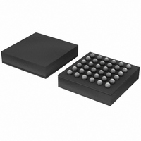
SC16C852VIET,115 NXP Semiconductors, SC16C852VIET,115 Datasheet - Page 28

SC16C852VIET,115
Manufacturer Part Number
SC16C852VIET,115
Description
IC UART DUAL W/FIFO 36TFBGA
Manufacturer
NXP Semiconductors
Datasheet
1.SC16C852VIBS557.pdf
(55 pages)
Specifications of SC16C852VIET,115
Features
Programmable
Number Of Channels
2, DUART
Fifo's
128 Byte
Protocol
RS485
Voltage - Supply
1.8V
With Auto Flow Control
Yes
With Irda Encoder/decoder
Yes
With False Start Bit Detection
Yes
With Modem Control
Yes
With Cmos
Yes
Mounting Type
Surface Mount
Package / Case
36-TFBGA
Transmitter And Receiver Fifo Counter
Yes
Data Rate
5Mbps
Mounting
Surface Mount
Operating Temperature (min)
-40C
Operating Temperature (max)
85C
Operating Temperature Classification
Industrial
Lead Free Status / RoHS Status
Lead free / RoHS Compliant
Other names
935282518115
SC16C852VIET-G
SC16C852VIET-G
SC16C852VIET-G
SC16C852VIET-G
Available stocks
Company
Part Number
Manufacturer
Quantity
Price
Company:
Part Number:
SC16C852VIET,115
Manufacturer:
NXP Semiconductors
Quantity:
10 000
NXP Semiconductors
SC16C852V
Product data sheet
7.5 Line Control Register (LCR)
The Line Control Register is used to specify the asynchronous data communication
format. The word length, the number of stop bits, and the parity are selected by writing the
appropriate bits in this register.
Table 16.
Table 17.
Table 18.
Table 19.
Bit
7
6
5:3
2
1:0
LCR[5]
X
X
0
0
1
LCR[2]
0
1
1
LCR[1]
0
0
1
1
Symbol
LCR[7]
LCR[6]
LCR[5:3]
LCR[2]
LCR[1:0]
LCR[4]
X
0
1
0
1
Line Control Register bits description
LCR[5:3] parity selection
LCR[2] stop bit length
LCR[1:0] word length
LCR[0]
0
1
0
1
Word length (bits)
5, 6, 7, 8
5
6, 7, 8
Dual UART with 128-byte FIFOs, IrDA, and XScale VLIO bus interface
All information provided in this document is subject to legal disclaimers.
LCR[3]
0
1
1
1
1
Stop bits. The length of stop bit is specified by this bit in conjunction with the
Word length bits 1, 0. These two bits specify the word length to be
Description
Divisor latch enable. The internal baud rate counter latch and Enhanced
Feature mode enable.
Set break. When enabled, the Break control bit causes a break condition to
be transmitted (the TX output is forced to a logic 0 state). This condition
exists until disabled by setting LCR[6] to a logic 0.
Programs the parity conditions (see
programmed word length (see
transmitted or received (see
Rev. 5 — 21 January 2011
logic 0 = divisor latch disabled (normal default condition)
logic 1 = divisor latch enabled
logic 0 = no TX break condition (normal default condition)
logic 1 = forces the transmitter output (TX) to a logic 0 for alerting the
remote receiver to a line break condition
logic 0 or cleared = default condition
logic 0 or cleared = default condition
Parity selection
no parity
odd parity
even parity
forced parity ‘1’
forced parity ‘0’
Stop bit length (bit times)
1
2
Word length (bits)
5
6
7
8
1
1
⁄
2
Table
Table
19).
Table
18).
17).
SC16C852V
© NXP B.V. 2011. All rights reserved.
28 of 55


