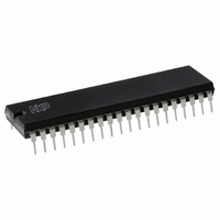
SCC68692C1N40,602 NXP Semiconductors, SCC68692C1N40,602 Datasheet - Page 20

SCC68692C1N40,602
Manufacturer Part Number
SCC68692C1N40,602
Description
IC DUART 40DIP
Manufacturer
NXP Semiconductors
Type
Dual asynchronous receiver/transmitter (DUART)r
Datasheet
1.SCC68692C1A44518.pdf
(28 pages)
Specifications of SCC68692C1N40,602
Number Of Channels
2, DUART
Package / Case
40-DIP (0.600", 15.24mm)
Features
False-start Bit Detection
Fifo's
3Bit
Voltage - Supply
5V
With Parallel Port
Yes
With Auto Flow Control
Yes
With False Start Bit Detection
Yes
With Cmos
Yes
Mounting Type
Through Hole
Data Rate
0.1152 MBd
Supply Voltage (max)
5.5 V
Supply Voltage (min)
4.5 V
Supply Current
10 mA
Maximum Operating Temperature
+ 70 C
Minimum Operating Temperature
0 C
Mounting Style
SMD/SMT
Operating Supply Voltage
5 V
Lead Free Status / RoHS Status
Lead free / RoHS Compliant
Lead Free Status / RoHS Status
Lead free / RoHS Compliant, Lead free / RoHS Compliant
Other names
933977610602
SCC68692C1N40
SCC68692C1N40
SCC68692C1N40
SCC68692C1N40
Philips Semiconductors
2004 Mar 03
NOTES:
1. INTRN or OP3 – OP7 when used as interrupt outputs.
2. The test for open-drain outputs is intended to guarantee switching of the output transistor. Measurement of this response is referenced from themidpoint of the switching signal, V
NOTE: DACKN low requires two rising edges of X1 clock after CSN is low.
Dual asynchronous receiver/transmitter (DUART)
point 0.5V above V
and can greatly affect the resultant measurement.
OL
. This point represents noise margin that assures true switching has occurred. Beyond this level, the effects of external circuitry and test environment are pronounced
DTACKN
X1/CLK
IACKN
D0–D7
INTRN
OP0–OP7
IP0–IP5
CSN
CSN
t
PS
INTERRUPT
OUTPUT
Figure 6. Interrupt Cycle Timing
t
t
CSC
DD
WRN
RDN
Figure 8. Interrupt Timing
OR
OLD DATA
1
Figure 7. Port Timing
t
DAL
20
t
DCR
t
CSD
V
t
M
IR
t
t
DAH
PH
t
V
PD
OL
t
DAT
V
+0.5V
OL
t
NEW DATA
DF
SD00150
SD00149
SCC68692
Product data
SD00090
M
, to a


