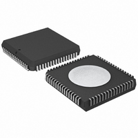
SC28L194A1A,512 NXP Semiconductors, SC28L194A1A,512 Datasheet - Page 30

SC28L194A1A,512
Manufacturer Part Number
SC28L194A1A,512
Description
IC UART QUAD W/FIFO 68-PLCC
Manufacturer
NXP Semiconductors
Datasheet
1.SC28L194A1BE528.pdf
(52 pages)
Specifications of SC28L194A1A,512
Features
False-start Bit Detection
Number Of Channels
4, QUART
Fifo's
16 Byte
Voltage - Supply
3.3V, 5V
With Auto Flow Control
Yes
With False Start Bit Detection
Yes
With Modem Control
Yes
With Cmos
Yes
Mounting Type
Surface Mount
Package / Case
68-LCC (J-Lead)
Lead Free Status / RoHS Status
Lead free / RoHS Compliant
Other names
568-1116-5
935261296512
SC28L194A1A
935261296512
SC28L194A1A
Available stocks
Company
Part Number
Manufacturer
Quantity
Price
Company:
Part Number:
SC28L194A1A,512
Manufacturer:
NXP Semiconductors
Quantity:
10 000
Philips Semiconductors
REGISTER MAPS
The registers of the SC28L194 are partitioned into two groups: those
used in controlling data channels and those used in handling the
actual data flow and status. Below is shown the general
configuration of all the register addressed. The “Register Map
Summary” shows the configuration of the lower four bits of the
address that is the same for the individual UARTs. It also shows the
REGISTER MAP SUMMARY
Table 43. Summary Register Map, Control
2006 Aug 15
0ccc 0000 (x00)
0ccc 0001 (x01)
0ccc 0010 (x02)
0ccc 0011 (x03)
0ccc 0100 (x04)
0ccc 0110 (x06)
0ccc 0111 (x07)
0ccc 1000 (x08)
0ccc 1001 (x09)
0ccc 1010 (x0A)
0ccc 1100 (x0C)
0000 1101 (x0D)
0ccc 1110 (x0E)
0000 1111 (x0F)
0001 1011 (x1B)
0001 1101 (x1D)
0001 1111 (x1F)
Quad UART for 3.3 V and 5 V supply voltage
Address (hex) ccc = channel
Mode Register 0 MR0a
Mode Register 1 MR1a
I/O Port Configuration Reg a I/OPCRa
Bid Control, Break Change
Bid Control, Change of State
Bid Control, Xon/Xoff
Bid Control, Address recognition
Xon Character Register
Xoff Character Register
Address Recognition Character
Receiver Clock Select Register
Transmitter Clock Select Register
Test Register
Global Chip Configuration Register
Interrupt Control Register
Watch-dog Timer Run Control
Interrupt Vector Register
Register Name
30
addresses for the several in the address space of UART A and
UART B that apply to the total chip configuration. The “Register Map
Detail” shows the use of every address in the 8-bit address space.
NOTE: The register maps for channels A and B (UARTs A and B)
contain some control registers that configure the entire chip. These
are denoted by a
symbol
Acronym
WDTRCR
BCRBRK
BCRCOS
XonCR
XoffCR
RxCSR
TxCSR
IOPCR
GCCR
BCRX
BCRA
ARCR
MR0
MR1
ICR
IVR
Reserved, set to 0
Read / Write
R/W
R/W
R/W
R/W
R/W
R/W
R/W
R/W
R/W
R/W
R/W
R/W
R/W
R/W
R/W
R/W
SC28L194
Product data sheet
Page
17
18
28
24
24
24
24
24
24
24
20
20
16
26
25
27


