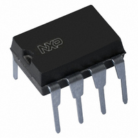
TDA7052A/N2,112 NXP Semiconductors, TDA7052A/N2,112 Datasheet - Page 6

TDA7052A/N2,112
Manufacturer Part Number
TDA7052A/N2,112
Description
IC AMP AUDIO 1.1W MONO AB 8DIP
Manufacturer
NXP Semiconductors
Type
Class ABr
Datasheet
1.TDA7052ATN2118.pdf
(12 pages)
Specifications of TDA7052A/N2,112
Output Type
1-Channel (Mono)
Package / Case
8-DIP (0.300", 7.62mm)
Max Output Power X Channels @ Load
1.1W x 1 @ 8 Ohm
Voltage - Supply
4.5 V ~ 18 V
Features
Depop, Mute, Short-Circuit and Thermal Protection, Volume Control
Mounting Type
Through Hole
Product
Class-AB
Output Power
1.1 W
Available Set Gain
35.5 dB
Thd Plus Noise
0.3 %
Operating Supply Voltage
5 V, 9 V, 12 V
Supply Current
7 mA
Maximum Power Dissipation
1250 mW
Maximum Operating Temperature
+ 85 C
Mounting Style
Through Hole
Audio Load Resistance
8 Ohms
Input Signal Type
Single
Minimum Operating Temperature
- 40 C
Output Signal Type
Differential
Supply Type
Single
Supply Voltage (max)
18 V
Supply Voltage (min)
4.5 V
Lead Free Status / RoHS Status
Lead free / RoHS Compliant
Lead Free Status / RoHS Status
Lead free / RoHS Compliant, Lead free / RoHS Compliant
Other names
568-1138-5
935054410112
TDA7052AN
935054410112
TDA7052AN
Available stocks
Company
Part Number
Manufacturer
Quantity
Price
Part Number:
TDA7052A/N2,112
Manufacturer:
NXP/恩智浦
Quantity:
20 000
Philips Semiconductors
CHARACTERISTICS
V
Notes to the characteristics
1. With a load connected to the outputs the quiescent current will increase, the maximum value of this increase being
2. The noise output voltage (RMS value) at f = 500 kHz is measured with R
3. The ripple rejection is measured with R
4. The noise output voltage (RMS value) is measured with R
July 1994
V
I
Maximum gain; V
P
THD
G
V
V
B
SVRR
Z
Minimum gain; V
G
V
Mute position
V
DC volume control
I
V
P
4
P
SYMBOL
I
P
O
I
no(rms)
no(rms)
O
1 W BTL mono audio amplifier with DC
volume control
v
v
off
= 6 V; T
equal to the DC output offset voltage dividend by R
is applied to the positive supply rail.
amb
positive supply voltage range
total quiescent current
output power
total harmonic distortion
voltage gain
input signal handling
noise output voltage (RMS value)
bandwidth
supply voltage ripple rejection
DC output offset voltage
input impedance (pin 2)
voltage gain
noise output voltage (RMS value)
output voltage in mute position
gain control range
control current
= 25 C; f = 1 kHz; TDA7052A: R
TDA7052A
TDA7052AT
TDA7052A
TDA7052AT
4
4
= 0.5 V
= 1.4 V
PARAMETER
S
= 0
L
= 8 ; TDA7052AT: R
and f = 100 Hz to 10 kHz. The ripple voltage of 200 mV, (RMS value)
V
note 1
THD = 10%
P
P
V
f = 500 kHz; note 2
note 3
note 4
V
V
1 dB
P
O
O
4
4
4
L
= 0.8 V; THD
= 0.4 V
= 6 V; R
= 0.5 W
= 0.25 W
.
0.3 V; V
6
CONDITIONS
S
= 5 k unweighted.
L
=
I
= 600 mV
L
1%
= 16 ; unless otherwise specified (see Fig.6).
S
= 0
and bandwidth = 5 kHz.
4.5
1.0
0.5
34.5
0.5
38
15
75
60
MIN.
7
1.1
0.55
0.3
0.3
35.5
0.65
210
20 Hz to
300 kHz
46
0
20
20
80
70
44
TDA7052A/AT
TYP.
Product specification
18
12
1
1
36.5
150
25
30
30
80
MAX. UNIT
V
mA
W
W
%
%
dB
V
dB
mV
k
dB
dB
V
V
V
A


