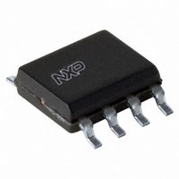
TDA8551T/N1,112 NXP Semiconductors, TDA8551T/N1,112 Datasheet - Page 7

TDA8551T/N1,112
Manufacturer Part Number
TDA8551T/N1,112
Description
IC AMP AUDIO PWR 1.4W MONO 8SOIC
Manufacturer
NXP Semiconductors
Type
Class ABr
Datasheet
1.TDA8551TN1112.pdf
(18 pages)
Specifications of TDA8551T/N1,112
Output Type
1-Channel (Mono)
Package / Case
8-SOIC (3.9mm Width)
Max Output Power X Channels @ Load
1.4W x 1 @ 8 Ohm
Voltage - Supply
2.7 V ~ 5.5 V
Features
Depop, Mute, Short-Circuit and Thermal Protection, Standby, Volume Control
Mounting Type
Surface Mount
Product
Class-AB
Output Power
1.4 W
Available Set Gain
20 dB
Thd Plus Noise
0.15 %
Operating Supply Voltage
5 V
Supply Current
6 mA
Maximum Power Dissipation
800 mW
Maximum Operating Temperature
+ 85 C
Mounting Style
SMD/SMT
Audio Load Resistance
8 Ohms
Input Signal Type
Single
Minimum Operating Temperature
- 40 C
Output Signal Type
Differential
Supply Type
Single
Supply Voltage (max)
5.5 V
Supply Voltage (min)
2.7 V
Lead Free Status / RoHS Status
Lead free / RoHS Compliant
Lead Free Status / RoHS Status
Lead free / RoHS Compliant, Lead free / RoHS Compliant
Other names
568-3477-5
935232730112
TDA8551TD
935232730112
TDA8551TD
NXP Semiconductors
Notes to the Characteristics
1. With a load connected at the outputs the quiescent current will increase, the maximum of this increase being equal
2. The DC output voltage with respect to ground is approximately 0.5V
3. Output voltage in mute position is measured with an input of 1 V (RMS), including noise, in a bandwidth of 20 kHz.
4. Total gain setting at +20 dB.
5. The noise output voltage is measured at the output in a frequency band from 20 Hz to 20 kHz (unweighted), input
6. Supply voltage ripple rejection is measured at the output, with a source impedance of R
1998 Feb 23
handbook, full pagewidth
1 W BTL audio amplifier with digital volume
control
The rise time (t
to the DC output offset voltage divided by R
source impedance R
The ripple voltage is a sine wave with frequency of 1 kHz and an amplitude of 100 mV (RMS) is applied to the positive
supply rail.
V UP/DOWN
V th(DOWN)
V float(max)
V float(min)
r
) and the width of the pulse (t
V th(UP)
V P
0
source
= 0 Ω.
t r
w
) are not critical.
t rep
Fig.3 Timing UP/DOWN pin.
L
.
t
t w
decreasing volume
7
increasing volume
floating
P
.
t r
t rep
source
t w
= 0 Ω at the input.
Product specification
MGK365
TDA8551


