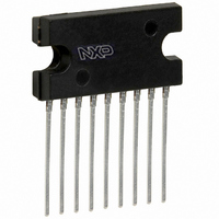
TDA1517/N3,112 NXP Semiconductors, TDA1517/N3,112 Datasheet - Page 7

TDA1517/N3,112
Manufacturer Part Number
TDA1517/N3,112
Description
IC AMP AUDIO PWR 6W MONO B 9SIL
Manufacturer
NXP Semiconductors
Type
Class Br
Datasheet
1.TDA1517N3112.pdf
(15 pages)
Specifications of TDA1517/N3,112
Output Type
2-Channel (Stereo)
Package / Case
9-SIL (Straight Leads)
Max Output Power X Channels @ Load
6W x 2 @ 4 Ohm
Voltage - Supply
6 V ~ 18 V
Features
Depop, Mute, Short-Circuit and Thermal Protection, Standby
Mounting Type
Through Hole
Product
Class-B
Output Power
6 W
Available Set Gain
20 dB
Thd Plus Noise
0.1 %
Operating Supply Voltage
14.4 V
Supply Current
40 mA
Maximum Power Dissipation
15000 mW
Maximum Operating Temperature
+ 85 C
Mounting Style
SMD/SMT
Audio Load Resistance
4 Ohms
Input Signal Type
Single
Minimum Operating Temperature
- 40 C
Output Signal Type
Single
Supply Type
Single
Supply Voltage (max)
18 V
Supply Voltage (min)
6 V
Lead Free Status / RoHS Status
Lead free / RoHS Compliant
Lead Free Status / RoHS Status
Lead free / RoHS Compliant, Lead free / RoHS Compliant
Other names
568-3501-5
935261847112
TDA1517U
935261847112
TDA1517U
NXP Semiconductors
AC CHARACTERISTICS
V
Notes
1. Output power is measured directly at the output pins of the IC.
2. Frequency response externally fixed.
3. Ripple rejection measured at the output with a source impedance of 0 Ω, maximum ripple amplitude of 2 V (p-p) and
4. Noise voltage measured in a bandwidth of 20 Hz to 20 kHz.
5. Noise output voltage independent of R
2004 Feb 18
P
THD
f
f
G
SVRR
|Z
V
α
|ΔG
P
lr
hr
cs
o
no
2 x 6 W stereo power amplifier
v
i
|
= 14.4 V; R
a frequency between 100 Hz and 10 kHz.
SYMBOL
v
|
L
= 4 Ω; f = 1 kHz; T
output power
total harmonic distortion
low frequency roll-off
high frequency roll-off
closed loop voltage gain
supply voltage ripple rejection
input impedance
noise output voltage
channel separation
channel unbalance
on
mute
standby
on
on
mute
PARAMETER
amb
= 25 °C; measured in Fig.6; unless otherwise specified.
s
(V
I
= 0 V).
THD = 0.5%; note 1
THD = 10%; note 1
P
at −3 dB; note 2
at −1 dB
note 3
R
R
note 5
R
o
s
s
s
= 1 W
= 0 Ω; note 4
= 10 Ω; note 4
= 10 Ω
CONDITIONS
7
4
5.5
−
−
20
19
48
48
80
50
−
−
−
40
−
MIN.
TDA1517; TDA1517P
5
6.0
0.1
45
−
20
−
−
−
60
50
70
50
−
0.1
TYP.
Product specification
−
−
−
−
−
21
−
−
−
75
−
100
−
−
1
MAX.
W
W
%
Hz
kHz
dB
dB
dB
dB
kΩ
μV
μV
μV
dB
dB
UNIT


