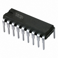
TDA1517P/N3,112 NXP Semiconductors, TDA1517P/N3,112 Datasheet - Page 5

TDA1517P/N3,112
Manufacturer Part Number
TDA1517P/N3,112
Description
IC AMP AUDIO PWR 6W STER 18HDIP
Manufacturer
NXP Semiconductors
Type
Class Br
Datasheet
1.TDA1517N3112.pdf
(15 pages)
Specifications of TDA1517P/N3,112
Output Type
2-Channel (Stereo)
Package / Case
18-DIP (0.300", 7.62mm) Exposed Pad
Max Output Power X Channels @ Load
6W x 2 @ 4 Ohm
Voltage - Supply
6 V ~ 18 V
Features
Depop, Mute, Short-Circuit and Thermal Protection, Standby
Mounting Type
Through Hole
Product
Class-B
Output Power
6 W
Available Set Gain
20 dB
Thd Plus Noise
0.1 %
Operating Supply Voltage
14.4 V
Supply Current
40 mA
Maximum Power Dissipation
15000 mW
Maximum Operating Temperature
+ 85 C
Mounting Style
Through Hole
Audio Load Resistance
4 Ohms
Input Signal Type
Single
Minimum Operating Temperature
- 40 C
Output Signal Type
Single
Supply Type
Single
Supply Voltage (max)
18 V
Supply Voltage (min)
6 V
Operational Class
Class-B
Audio Amplifier Output Configuration
2-Channel Stereo
Output Power (typ)
6x2@4OhmW
Audio Amplifier Function
Speaker
Total Harmonic Distortion
0.1@4Ohm@1W%
Single Supply Voltage (typ)
14.4V
Dual Supply Voltage (typ)
Not RequiredV
Power Supply Requirement
Single
Power Dissipation
15W
Rail/rail I/o Type
No
Power Supply Rejection Ratio
80dB
Single Supply Voltage (min)
6V
Single Supply Voltage (max)
18V
Dual Supply Voltage (min)
Not RequiredV
Dual Supply Voltage (max)
Not RequiredV
Operating Temp Range
-40C to 85C
Operating Temperature Classification
Industrial
Mounting
Through Hole
Pin Count
18
Lead Free Status / RoHS Status
Lead free / RoHS Compliant
Lead Free Status / RoHS Status
Lead free / RoHS Compliant, Lead free / RoHS Compliant
Other names
568-1128-5
935261850112
TDA1517PN
935261850112
TDA1517PN
NXP Semiconductors
LIMITING VALUES
In accordance with the Absolute Maximum Rating System (IEC 60134).
THERMAL RESISTANCE
2004 Feb 18
handbook, halfpage
V
V
V
ERG
I
I
P
T
T
T
R
R
R
OSM
ORM
SYMBOL
SYMBOL
stg
amb
c
P
P(sc)
P(r)
tot
2 x 6 W stereo power amplifier
th(j-c)
th(j-p)
th(j-a)
(1) R
(2) R
(W)
O
P
18
12
th j-c
th j-p
6
0
25
= 8 K/W.
= 15 K/W.
supply voltage
AC and DC short-circuit safe voltage
reverse polarity
energy handling capability at outputs
non-repetitive peak output current
repetitive peak output current
total power dissipation
storage temperature
operating ambient temperature
crystal temperature
TDA1517/N3; TDA1517/N3/S5 thermal resistance from junction to case
TDA1517P
TDA1517/N3; TDA1517/N3/S5;
TDA1517P
0
Fig.4 Power derating curve.
TYPE NUMBER
50
(2)
PARAMETER
(1)
100
T
amb
( C)
o
150
MLC354
thermal resistance from junction to pins
thermal resistance from junction to
ambient
operating
no signal
V
see Fig.4
P
= 0 V
5
PARAMETER
CONDITIONS
TDA1517; TDA1517P
−
−
−
−
−
−
−
−
−55
−40
−
MIN.
VALUE
15
50
8
Product specification
18
20
18
6
200
4
2.5
15
+150
+85
150
MAX.
UNIT
K/W
K/W
K/W
V
V
V
V
mJ
A
A
W
°C
°C
°C
UNIT


